
Datasheet

LT3748
17
3748fb
For more information www.linear.com/LT3748
applications inForMation
(over manufacturing variations), this can be accommodated
by adjusting the R
FB
/R
REF
resistor ratio.
Winding Resistance Effects
Resistance in either the primary or secondary will reduce
overall efficiency (P
OUT
/P
IN
). Good output voltage regula-
tion will be maintained independent of winding resistance
due to the boundar
y mode operation of the LT3748.
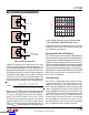
Bifilar Winding
A bifilar, or similar winding technique, is a good way to
minimize troublesome leakage inductances. However, re
-
member that
this will also increase primary-to-secondary
capacitance
and limit the primary-to-secondary breakdown
voltage, so, bifilar winding is not always practical. The
Linear Technology Applications group is available and
extremely qualified to assist in the selection and/or design
of the transformer.
Selecting a Current Sense Resistor
The external current sense resistor allows the user to
optimize the current limit behavior for the particular ap
-
plication under consideration. As the current sense resistor
is varied from several ohms down to tens of milliohms,
peak switch current goes from a fraction of an ampere
to tens of amperes. Care must be taken to ensure proper
circuit operation, especially with small current sense
resistor values.
For example, a peak MOSFET switch current of 4A
requires
a sense resistor of 0.025Ω. Note that the instantaneous
peak power in the sense resistor is 1W, and it must be
rated accordingly. The LT3748 has only a single sense line
to this resistor. Therefore, any parasitic resistance in the
ground side connection of the sense resistor will increase
its apparent value. In the case of a 0.025Ω sense resistor,
1mΩ of parasitic resistance will cause a 4% reduction in
peak switch current. Therefore, resistance of printed circuit
copper traces and vias cannot necessarily be ignored.
Another issue for proper operation of the current sense
circuitry is avoiding prematurely tripping the SENSE
threshold while slewing the MOSFET drain when the GATE
pin goes high. The LT3748 does not begin to compare
the SENSE pin voltage with the target threshold until the
GATE pin is near its final value, or until at least 150ns
has passed, whichever occurs more slowly. This should
be entirely sufficient for most applications but premature
tripping of the SENSE comparator may occur in cases
where a MOSFET with very high Q
G
is used with a series
resistor at the GATE pin.
Output Short Circuits and SENSE Pin Over Current
The LT3748 has an internal threshold to
detect when
primary inductor current exceeds the programmed range.
This can result from an inductive output short-circuit and
an output voltage below zero, reflecting a voltage back to
the primary side of the transformer which, in turn, causes
the LT3748 to turn the external MOSFET on before the
secondary current has discharged. When the voltage at
the SENSE pin exceeds approximately 130mV—equiva
-
lent to
30%
higher than the programmed I
LIM(MAX)
in
the R
SENSE
resistor—the SS pin will be reset, stopping
switching. Once the soft-start capacitor is recharged and
the soft-start threshold is reached, switching will resume
at the minimum current limit.
High Drain Capacitance and Low Current Operation
When designing applications with some combination of a
low current limit (I
LIM
< 1A), a high secondary-to-primary
turns ratio (N
PS
<< 1), multiple output windings, or very
capacitive output diodes, it is important to minimize the
capacitance reflected onto the primary winding and on the
drain of the external MOSFET. After the MOSFET turns off
during each switching cycle, the primary current charges
that capacitance to slew the MOSFET drain until the second
-
ary begins to deliver power, and if the drain node does not
slew and remain above V
IN
within approximately 200ns
once the GATE pin goes low and the MOSFET turns off,
the LT3748 may detect that the current in the secondary
is zero and turn the MOSFET back on prematurely, caus
-
ing the LT3748 to switch continuously while delivering
ver
y little power to the output. The result will be droop of
the output voltage at lighter loads and oscillation at the
V
C
node. This problem can be prevented by maximizing
N
PS
(minimizing ratio of secondary windings to primary
windings), increasing the peak drain current (minimizing
R
SENSE
), and minimizing the output diode and transformer
capacitance.
Downloaded from Arrow.com.Downloaded from Arrow.com.Downloaded from Arrow.com.Downloaded from Arrow.com.Downloaded from Arrow.com.Downloaded from Arrow.com.Downloaded from Arrow.com.Downloaded from Arrow.com.Downloaded from Arrow.com.Downloaded from Arrow.com.Downloaded from Arrow.com.Downloaded from Arrow.com.Downloaded from Arrow.com.Downloaded from Arrow.com.Downloaded from Arrow.com.Downloaded from Arrow.com.Downloaded from Arrow.com.