
Datasheet


LT3756/LT3756-1/LT3756-2
12
375612fb
applicaTions inForMaTion
When V
CTRL
is higher than 1.2V, the LED current is regu-
lated to:
I
LED
=
100mV
R
LED
The LED current programming feature can increase total
dimming range by a factor of 10. The CTRL pin should
not be left open (tie to V
REF
if not used). The CTRL pin
can also be used in conjunction with a thermistor to
provide overtemperature protection for the LED load, or
with a resistor divider to V
IN
to reduce output power and
switching current when V
IN
is low. The presence of a time
varying differential voltage signal (ripple) across ISP and
ISN at the switching frequency is expected. The amplitude
of this signal is increased by high LED load current, low
switching frequency and/or a smaller value output filter
capacitor. Some level of ripple signal is acceptable: the
compensation capacitor on the VC pin filters the signal so
the average difference between ISP and ISN is regulated
to the user-programmed value. Ripple voltage amplitude
(peak-to-peak) in excess of 20mV should not cause mis-
operation, but may lead to noticeable offset between the
average value and the user-programmed value.
Programming Output Voltage (Constant-Voltage
Regulation) or Open LED/Overvoltage Threshold
For a boost or SEPIC application, the output voltage can
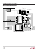
be set by selecting the values of R3 and R4 (see Figure 2)
according to the following equation:
V
OUT
= 1.25 •
R3 + R4
R4
For a boost type LED driver, set the resistor from the output
to the FB pin such that the expected V
FB
during normal
FB
LT3756
V
IN
R4
375612 F02
R3
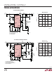
Figure 2. Feedback Resistor Connection
for Boost or SEPIC LED Drivers
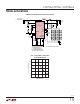
FB
LT3756
100k
V
OUT
R4
375612 F03
R3
LED
ARRAY
R
SEN(EXT)
C
OUT
+
–
Figure 3. Feedback Resistor Connection for
Buck Mode or Buck-Boost Mode LED Driver
operation will not exceed 1.1V. For an LED driver of buck or
a buck-boost configuration, the output voltage is typically
level-shifted to a signal with respect to GND as illustrated
in Figure 3. The output can be expressed as:
V
OUT
= V
BE
+ 1.25 •
R3
R4
ISP/ISN Short-Circuit Protection Feature (for SEPIC)
The ISP and ISN pins have a protection feature indepen-
dent of the LED current sense feature that operates at
ISN below 3V. The purpose of this feature is to provide
continuous current sensing when ISN is below the LED
current sense common mode range (during start-up or
an output short-circuit fault) to prevent the development
of excessive switching currents that could damage the
power components in a SEPIC converter. The action
threshold (150mV, typ) is above the default LED current
sense threshold, so that no interference will occur over
the ISN voltage range where these two functions overlap.
This feature acts in the same manner as SENSE current
limit— it prevents GATE from going high (switch turn-on)
until the ISP/ISN difference falls below the threshold. If the
load has appreciable series inductance, use of a Schottky
clamp from GND to ISN is recommended for the SEPIC
to prevent excessive current flowing from the ISN pin in
a fault.
Dimming Control
There are two methods to control the current source for
dimming using the LT3756. One method uses the CTRL
pin to adjust the current regulated in the LEDs. A second