
Datasheet

LT3791-1
18
37911f
Soft-Start
Soft-start reduces the input power sources’ surge currents
by gradually increasing the controller’s current limit (pro-
portional to an internally buffered clamped equivalent of
V
C
). The soft-start interval is set by the soft-start capacitor
selection according to the following equation
t
SS
=
1.2V
14µA
• C
SS
A 100k resistor must be placed between SS and V
REF
for
the LT3791-1. This 100k resistor also contributes the extra
SS charge current. Make sure C
SS
is large enough when
there is loading during start-up.
Loop Compensation
The LT3791-1 uses an internal transconductance error
amplifier whose V
C
output compensates the control loop.
The external inductor, output capacitor and the compensa-
tion resistor and capacitor determine the loop stability.
The inductor and output capacitor are chosen based on
performance, size and cost. The compensation resistor and
capacitor at V
C
are set to optimize control loop response
and stability. For typical applications, a 10nF compensation
capacitor at V
C
is adequate, and a series resistor should
always be used to increase the slew rate on the V
C
pin to
maintain tighter regulation of output current during fast
transients on the input supply of the converter.
Power MOSFET Selections and Efficiency
Considerations
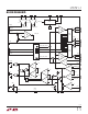
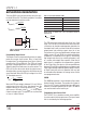
The LT3791-1 requires four external N-channel power
MOSFETs, two for the top switches (switch M1 and M4,
shown in Figure 1) and two for the bottom switches (switch
M2 and M3 shown in Figure 1). Important parameters for
the power MOSFETs are the breakdown voltage, V
BR(DSS)
,
threshold voltage, V
GS(TH)
, on-resistance, R
DS(ON)
, reverse
transfer capacitance, C
RSS
, and maximum current, I
DS(MAX)
.
The drive voltage is set by the 5V INTV
CC
supply. Con-
sequently, logic-level threshold MOSFETs must be used
in LT3791-1 applications. If the input voltage is expected
to drop below the 5V, then sub-logic threshold MOSFETs
should be considered.
In order to select the power MOSFETs, the power dis-
sipated by the device must be known. For switch M1, the
maximum power dissipation happens in boost operation,
when it remains on all the time. Its maximum power dis-
sipation at maximum output current is given by:
P
M1(BOOST)
=
I
LED
• V
OUT
V
IN
2
• ρ
T
•R
DS(ON)
where ρ
T
is a normalization factor (unity at 25°C)
accounting for the significant variation in on-resistance
with temperature, typically 0.4%/°C as shown in Figure10.
For a maximum junction temperature of 125°C, using a
value of ρ
T
= 1.5 is reasonable.
Switch M2 operates in buck operation as the synchronous
rectifier. Its power dissipation at maximum output current
is given by:
P
M2(BUCK)
=
V
IN
– V
OUT
V
IN
•I
LED
2
• ρ
T
•R
DS(ON)
Switch M3 operates in boost operation as the control
switch. Its power dissipation at maximum current is
given by:
P
M3(BOOST)
=
V
OUT
– V
IN
( )
• V
OUT
V
IN
2
•I
LED
2
• ρ
T
•R
DS(ON)
+ k • V
OUT
3
•
I
LED
V
IN
• C
RSS
• f
where C
RSS
is usually specified by the MOSFET manufac-
turers. The constant k, which accounts for the loss caused
by reverse-recovery current, is inversely proportional to
the gate drive current and has an empirical value of 1.7.
For switch M4, the maximum power dissipation happens
in boost operation, when its duty cycle is higher than
50%. Its maximum power dissipation at maximum output
current is given by:
P
M4(BOOST)
=
V
IN
V
OUT
•
I
LED
• V
OUT
V
IN
2
• ρ
T
•R
DS(ON)
For the same output voltage and current, switch M1 has
the highest power dissipation and switch M2 has the low-
est power dissipation unless a short occurs at the output.
applicaTions inForMaTion