
Datasheet

LT3956
12
3956f
applicaTions inForMaTion
Dimming Control
There are two methods to control the current source for
dimming using the LT3956. One method uses the CTRL
pin to adjust the current regulated in the LEDs. A second
method uses the PWM pin to modulate the current source
between zero and full current to achieve a precisely pro-
grammed average current. To make this method of current
control more accurate, the switch demand current is stored
on the V
C
node during the quiescent phase when PWM is
low. This feature minimizes recovery time when the PWM
signal goes high. To further improve the recovery time, a
disconnect switch may be used in the LED current path to
prevent the ISP node from discharging during the PWM
signal low phase. The minimum PWM on or off time will
depend on the choice of operating frequency through the
R
T
input. For best overall performance, the minimum PWM
low or high time should be at least six switching cycles
(6μs for f
SW
= 1MHz).
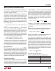
Programming the Switching Frequency
The R
T
frequency adjust pin allows the user to program
the switching frequency from 100kHz to 1MHz to optimize
efficiency/performance or external component size. Higher
frequency operation yields smaller component size but
increases switching losses and gate driving current, and
may not allow sufficiently high or low duty cycle operation.
Lower frequency operation gives better performance at the
cost of larger external component size. For an appropriate
R
T
resistor value see Table 1. An external resistor from the
RT pin to GND is required—do not leave this pin open.
Table 1. Switching Frequency vs R
T
Value
f
OSC
(kHz) R
T
(k)
1000 10
900 11.8
800 13
700 15.4
600 17.8
500 21
400 26.7
300 35.7
200 53.6
100 100
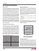
Duty Cycle Considerations
Switching duty cycle is a key variable defining converter
operation, therefore, its limits must be considered when
programming the switching frequency for a particular
application. The fixed minimum on-time and minimum
off-time (see Figure 4) and the switching frequency define
the minimum and maximum duty cycle of the switch,
respectively. The following equations express the mini-
mum/maximum duty cycle:
Min Duty Cycle = (minimum on-time) • switching
frequency
Max Duty Cycle = 1 – (minimum off-time) • switching
frequency
When calculating the operating limits, the typical values
for on/off-time in the data sheet should be increased by at
least 60ns to allow margin for PWM control latitude and
SW node rise/fall times.
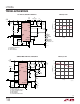
0
100
200
300
50
150
250
3956 F04
TIME (ns)
TEMPERATURE (°C)
–50 0
50
75
–25
25
100
125
MINIMUM ON-TIME
MINIMUM OFF-TIME
Figure 4. Typical Switch Minimum On
and Off Pulse Width vs Temperature
Thermal Considerations
The LT3956 is rated to a maximum input voltage of 80V.
Careful attention must be paid to the internal power dis-
sipation of the IC at higher input voltages to ensure that a
junction temperature of 125°C is not exceeded. This junction
limit is especially important when operating at high ambient
temperatures. If the LT3956’s junction temperature reaches
165°C (typ), the power switch will be turned off and the
soft-start (SS) pin will be discharged to GND. Switching