
Datasheet

LT3970 Series
13
3970fc
operation, the noise is typically very quiet to a casual ear.
If this is unacceptable, use a high performance tantalum
or electrolytic capacitor at the output.
A final precaution regarding ceramic capacitors concerns
the maximum input voltage rating of the LT3970. As pre
-
viously mentioned, a ceramic input capacitor combined
with trace or cable inductance forms a high quality (under
damped) tank circuit. If the L
T3970 circuit is plugged into a
live supply, the input voltage can ring to twice its nominal
value, possibly exceeding the LT3970’s rating. This situation
is easily avoided (see the Hot Plugging Safely section).
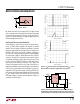
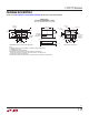
Low Ripple Burst Mode Operation
To enhance efficiency at light loads, the LT3970 operates
in low ripple Burst Mode operation which keeps the output
capacitor charged to the proper voltage while minimizing
the input quiescent current. During Burst Mode opera
-
tion, the LT3970 delivers single cycle bursts of current to
the output capacitor followed by sleep periods where the
output power is delivered to the load by the output capaci
-
tor. Because the LT3970 delivers power to the output with
single, low current pulses, the output ripple is kept below
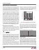
5mV for a typical application. See Figure 2.
As the load current decreases towards a no load condition,
the per
centage of time that the L
T3970 operates in sleep
mode increases and the average input current is greatly
reduced resulting in high efficiency even at very low loads.
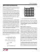
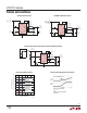
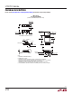
Note that during Burst Mode operation, the switching
frequency will be lower than the programmed switching
frequency. See Figure 3.
At higher output loads (above ~45mA for the front page
application) the LT3970 will be running at the frequency
programmed by the R
T
resistor, and will be operating in
standard PWM mode. The transition between PWM and
low ripple Burst Mode is seamless, and will not disturb
the output voltage.
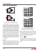
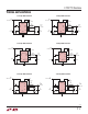
BOOST and BD Pin Considerations
Capacitor C3 and the internal boost Schottky diode (see the
Block Diagram) are used to generate a boost voltage that
is higher than the input voltage. In most cases a 0.22µF
capacitor will work well. Figure 4 shows two ways to ar
-
range the boost circuit. The BOOST pin must be more than
1.9V above the SW pin for best efficiency. For outputs of
2.2V and above, the standard circuit (Figure 4a) is best.
For outputs between 2.2V and 2.5V, use a 0.47µF boost
capacitor. For output voltages below 2.2V, the boost diode
can be tied to the input (Figure 4b), or to another external
supply greater than 2.2V. However, the circuit in Figure 4a
is more efficient because the BOOST pin current and BD
pin quiescent current come from a lower voltage source.
Also, be sure that the maximum voltage ratings of the
BOOST and BD pins are not exceeded.
The minimum operating voltage of an LT3970 application
is limited by the minimum input voltage (4.2V) and by the
maximum duty cycle as outlined in a previous section. For
output voltages greater than 3.4V, the minimum input volt
-
age is also limited by the boost circuit for proper start-up.
applicaTions inFormaTion
Figure 2. Burst Mode Operation
Figure 3. Switching Frequency in Burst Mode Operation
V
OUT
5mV/DIV
V
SW
5V/DIV
I
L
100mA/DIV
2µs/DIV
FRONT PAGE APPLICATION
V
IN
= 12V
V
OUT
= 5V
I
LOAD
= 10mA
3970 F02
LOAD CURRENT (mA)
0
400
500
700
150 250
3070 F03
300
200
50 100
200 300 350
100
0
600
SWITCHING FREQUENCY (kHz)
FRONT PAGE APPLICATION