
Datasheet

LT3971/LT3971-3.3/LT3971-5
14
3971fd
maximum load current. For details of maximum output cur-
rent and discontinuous operation, see Linear Technology’s
Application Note 44. Finally, for duty cycles greater than
50% (V
OUT
/V
IN
>0.5), a minimum inductance is required to
avoid sub-harmonic oscillations. See Application Note 19.
One approach to choosing the inductor is to start with
the simple rule given above, look at the available induc-
tors, and choose one to meet cost or space goals. Then
use the equations above to check that the LT3971 will be
able to deliver the required output current. Note again
that these equations assume that the inductor current is
continuous. Discontinuous operation occurs when I
OUT
is less than ΔI
L
/2.
Input Capacitor
Bypass the input of the LT3971 circuit with a ceramic
capacitor of X7R or X5R type. Y5V types have poor
performance over temperature and applied voltage, and
should not be used. A 4.7μF to 10μF ceramic capacitor
is adequate to bypass the LT3971 and will easily handle
the ripple current. Note that larger input capacitance is
required when a lower switching frequency is used (due
to longer on-times). If the input power source has high
impedance, or there is significant inductance due to
long wires or cables, additional bulk capacitance may be
necessary. This can be provided with a low performance
electrolytic capacitor.
Step-down regulators draw current from the input sup-
ply in pulses with very fast rise and fall times. The input
capacitor is required to reduce the resulting voltage
ripple at the LT3971 and to force this very high frequency
switching current into a tight local loop, minimizing EMI.
A 4.7μF capacitor is capable of this task, but only if it is
placed close to the LT3971 (see the PCB Layout section).
A second precaution regarding the ceramic input capacitor
concerns the maximum input voltage rating of the LT3971.
A ceramic input capacitor combined with trace or cable
inductance forms a high quality (under damped) tank
circuit. If the LT3971 circuit is plugged into a live supply,
the input voltage can ring to twice its nominal value, pos-
sibly exceeding the LT3971’s voltage rating. This situation
is easily avoided (see the Hot Plugging Safely section).
Output Capacitor and Output Ripple
The output capacitor has two essential functions. Along
with the inductor, it filters the square wave generated by the
LT3971 to produce the DC output. In this role it determines
the output ripple, so low impedance (at the switching
frequency) is important. The second function is to store
energy in order to satisfy transient loads and stabilize the
LT3971’s control loop. Ceramic capacitors have very low
equivalent series resistance (ESR) and provide the best
ripple performance. A good starting value is:
C
OUT
=
100
V
OUT
f
SW
where f
SW
is in MHz, and C
OUT
is the recommended output
capacitance in μF. Use X5R or X7R types. This choice will
provide low output ripple and good transient response.
Transient performance can be improved with a higher
value capacitor. Increasing the output capacitance will
also decrease the output voltage ripple. A lower value of
output capacitor can be used to save space and cost but
transient performance will suffer.
When choosing a capacitor, look carefully through the
data sheet to find out what the actual capacitance is under
operating conditions (applied voltage and temperature). A
physically larger capacitor or one with a higher voltage rating
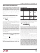
may be required. Table 3 lists several capacitor vendors.
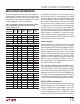
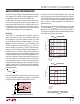
Table 3. Recommended Ceramic Capacitor Vendors
MANUFACTURER WEBSITE
AVX www.avxcorp.com
Murata www.murata.com
Taiyo Yuden www.t-yuden.com
Vishay Siliconix www.vishay.com
TDK www.tdk.com
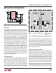
Catch Diode Selection
The catch diode (D1 from Block Diagram) conducts cur-
rent only during switch off time. Average forward current
in normal operation can be calculated from:
I
D(AVG)
=I
OUT
V
IN
– V
OUT
V
IN
where I
OUT
is the output load current. The only reason to
consider a diode with a larger current rating than necessary
APPLICATIONS INFORMATION