
Datasheet

LT3971/LT3971-3.3/LT3971-5
19
3971fd
APPLICATIONS INFORMATION
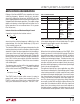
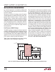
PCB Layout
For proper operation and minimum EMI, care must be taken
during printed circuit board layout. Figure 9 shows the
recommended component placement with trace, ground
plane and via locations. Note that large, switched currents
flow in the LT3971’s V
IN
and SW pins, the catch diode
(D1), and the input capacitor (C1). The loop formed by
these components should be as small as possible. These
components, along with the inductor and output capacitor,
should be placed on the same side of the circuit board,
and their connections should be made on that layer. Place
a local, unbroken ground plane below these components.
The SW and BOOST nodes should be as small as possible.
Finally, keep the FB and R
T
nodes small so that the ground
traces will shield them from the SW and BOOST nodes.
The Exposed Pad on the bottom of the package must be
soldered to ground so that the pad acts as a heat sink. To
keep thermal resistance low, extend the ground plane as
much as possible, and add thermal vias under and near
the LT3971 to additional ground planes within the circuit
board and on the bottom side.
Hot Plugging Safely
The small size, robustness and low impedance of ceramic
capacitors make them an attractive option for the input
bypass capacitor of LT3971 circuits. However, these ca-
pacitors can cause problems if the LT3971 is plugged into
a live supply. The low loss ceramic capacitor, combined
with stray inductance in series with the power source,
forms an under damped tank circuit, and the voltage at
the V
IN
pin of the LT3971 can ring to twice the nominal
input voltage, possibly exceeding the LT3971’s rating and
damaging the part. If the input supply is poorly controlled
or the user will be plugging the LT3971 into an energized
supply, the input network should be designed to prevent
this overshoot. See Linear Technology Application Note
88 for a complete discussion.
High Temperature Considerations
For higher ambient temperatures, care should be taken in
the layout of the PCB to ensure good heat sinking of the
LT3971. The Exposed Pad on the bottom of the package
must be soldered to a ground plane. This ground should be
tied to large copper layers below with thermal vias; these
layers will spread heat dissipated by the LT3971. Placing
additional vias can reduce thermal resistance further. The
maximum load current should be derated as the ambient
temperature approaches the maximum junction rating.
Power dissipation within the LT3971 can be estimated by
calculating the total power loss from an efficiency measure-
ment and subtracting the catch diode loss and inductor
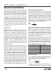
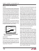
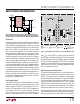
Figure 8. Diode D4 Prevents a Shorted Input from Discharging a
Backup Battery Tied to the Output. It Also Protects the Circuit from
a Reversed Input. The LT3971 Runs Only When the Input is Present
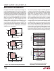
Figure 9. A Good PCB Layout Ensures Proper, Low EMI Operation
LT3971
BOOSTV
IN
EN
V
IN
V
OUT
BACKUP
3971 F07
SW
BD
D4
MBRS140
FBGND
+
VIAS TO LOCAL GROUND PLANE
VIAS TO V
OUT
VIAS TO RUN/SS
VIAS TO PG
VIAS TO V
IN
OUTLINE OF LOCAL
GROUND PLANE
3971 F09
L1
C2
V
OUT
D1
C1
C3
C5
C4
R1
R2
R
T
R
PG
GND
GND
VIAS TO SYNC