
Datasheet

LT3971/LT3971-3.3/LT3971-5
13
3971fd
Ratings of the V
IN
and BOOST pins, regardless of chosen
switching frequency. However, during such transients
where V
IN
is higher than V
IN(OP-MAX)
, the LT3971 will enter
pulse-skipping operation where some switching pulses are
skipped to maintain output regulation. The output voltage
ripple and inductor current ripple will be higher than in
typical operation. Do not overload when V
IN
is greater
than V
IN(OP-MAX)
.
Inductor Selection and Maximum Output Current
A good first choice for the inductor value is:
L =
V
OUT
+ V
D
f
SW
where f
SW
is the switching frequency in MHz, V
OUT
is the
output voltage, V
D
is the catch diode drop (~0.5V) and L
is the inductor value in μH.
The inductor’s RMS current rating must be greater than the
maximum load current and its saturation current should be
about 30% higher. For robust operation in fault conditions
(start-up or short-circuit) and high input voltage (>30V),
the saturation current should be above 3.8A. To keep the
efficiency high, the series resistance (DCR) should be less
than 0.1Ω, and the core material should be intended for
high frequency applications. Table 2 lists several vendors
and suitable types.
The inductor value must be sufficient to supply the desired
maximum output current (I
OUT(MAX)
), which is a function
of the switch current limit (I
LIM
) and the ripple current.
I
OUT(MAX)
=I
LIM
–
ΔI
L
2
The LT3971 limits its peak switch current in order to
protect itself and the system from overload faults. The
LT3971’s switch current limit (I
LIM
) is at least 2.4A at low
duty cycles and decreases linearly to 1.75A at DC = 0.8.
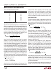
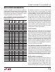
Table 2. Inductor Vendors
VENDOR URL PART SERIES TYPE
Murata www.murata.com LQH55D Open
TDK www.componenttdk.com SLF7045
SLF10145
Shielded
Shielded
Toko www.toko.com D62CB
D63CB
D73C
D75F
Shielded
Shielded
Shielded
Open
Coilcraft www.coilcraft.com MSS7341
MSS1038
Shielded
Shielded
Sumida www.sumida.com CR54
CDRH74
CDRH6D38
CR75
Open
Shielded
Shielded
Open
When the switch is off, the potential across the inductor
is the output voltage plus the catch diode drop. This gives
the peak-to-peak ripple current in the inductor:
ΔI
L
=
(1− DC) • (V
OUT
+ V
D
)
L • f
SW
Where f
SW
is the switching frequency of the LT3971, DC is
the duty cycle and L is the value of the inductor. Therefore,
the maximum output current that the LT3971 will deliver
depends on the switch current limit, the inductor value,
and the input and output voltages. The inductor value may
have to be increased if the inductor ripple current does
not allow sufficient maximum output current (I
OUT(MAX)
)
given the switching frequency, and maximum input voltage
used in the desired application.
The optimum inductor for a given application may differ
from the one indicated by this simple design guide. A larger
value inductor provides a higher maximum load current
and reduces the output voltage ripple. If your load is lower
than the maximum load current, than you can relax the
value of the inductor and operate with higher ripple cur-
rent. This allows you to use a physically smaller inductor,
or one with a lower DCR resulting in higher efficiency. Be
aware that if the inductance differs from the simple rule
above, then the maximum load current will depend on
the input voltage. In addition, low inductance may result
in discontinuous mode operation, which further reduces
APPLICATIONS INFORMATION