
Datasheet


LT3995
20
3995f
For more information www.linear.com/LT3995
output current at the frequency set by the R
T
resistor (see
Inductor Selection section). The slope compensation is set
by the R
T
value, while the minimum slope compensation
required to avoid subharmonic oscillations is established
by the inductor size, input voltage and output voltage.
Since the synchronization frequency will not change the
slopes of the inductor current waveform, if the inductor
is large enough to avoid subharmonic oscillations at the
frequency set by R
T
, than the slope compensation will be
sufficient for all synchronization frequencies.
Power Good Flag
The PG pin is an open-drain output which is used to indicate
to the user when the output voltage is within regulation.
When the output is lower than the regulation voltage by
more than 8.4%, as determined from the FB pin voltage,
the PG pin will pull low to indicate the power is not good.
Otherwise, the PG pin will go high impedance and can
be pulled logic high with a resistor pull-up. The PG pin is
only comparing the output voltage to an accurate refer-
ence when the LT3995 is enabled and V
IN
is above 4.3V.
When the part is shutdown, the PG is actively pulled low to
indicate that the LT3995 is not regulating the output. The
input voltage must be greater than 1.4V to fully turn-on
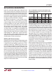
the active pull-down device. Figure 8 shows the status of
the PG pin as the input voltage is increased.
APPLICATIONS INFORMATION
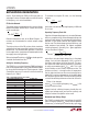
Figure 8. PG Pin Voltage Versus Input Voltage when PG
Is Connected to 3V Through a 150k Resistor. The FB Pin
Voltage Is 1.15V
INPUT VOLTAGE (V)
0
PG PIN VOLTAGE (V)
2
3
4
3995 F08
1
0
1
2
2.5
5
4
3
0.5
1.5
4.5
3.5
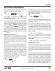
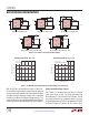
V
IN
BOOST
V
IN
EN
3995 F09
V
OUT
BACKUP
LT3995
D4
PDS360
SW
OUT
GND FB
+
Figure 9. Diode D4 Prevents a Shorted Input from Discharging
a Backup Battery Tied to the Output. It Also Protects the Circuit
from a Reversed Input. The LT3995 Runs Only When the Input
Is Present
Shorted and Reversed Input Protection
If the inductor is chosen so that it won’t saturate excessively,
a LT3995 buck regulator will tolerate a shorted output and
the power dissipation will be limited by current limit fold-
back (see Current Limit Foldback and Thermal Protection
section). There is another situation to consider in systems
where the output will be held high when the input to the
LT3995 is absent. This may occur in battery charging ap-
plications or in battery backup systems where a battery
or some other supply is diode ORed with the LT3995’s
output. If the V
IN
pin is allowed to float and the EN/UVLO
pin is held high (either by a logic signal or because it is
tied to V
IN
), then the LT3995’s internal circuitry will pull its
quiescent current through its SW pin. This is fine if your
system can tolerate a few μA in this state. If you ground
the EN pin, the SW pin current will drop to essentially
zero. However, if the V
IN
pin is grounded while the output
is held high, regardless of EN, parasitic diodes inside the
LT3995 can pull current from the output through the SW
pin and the V
IN
pin. Figure 9 shows a circuit that will run
only when the input voltage is present and that protects
against a shorted or reversed input.