
Datasheet


LT4275
7
4275f
applicaTions inForMaTion
Table 1. Classification Codes, Power Levels and Resistor Selection
CLASS
PD POWER
AVAILABLE PD TYPE
NOMINAL CLASS
CURRENT
LT4275 GRADE CAPABILITY RESISTOR
A B C R
CLS
R
CLS
++
0 13W Type 1 <0.4mA
Open Open
1 3.84W Type 1 10.5mA
140Ω Open
2 6.49W Type 1 18.5mA
76.8Ω Open
3 13W Type 1 28mA
49.9Ω Open
4 25.5W Type 2 40mA
34.8Ω Open
4* 38.7W LTPoE
++
40mA
Open 34.8Ω
4* 52.7W LTPoE
++
40mA
140Ω 46.4Ω
4* 70W LTPoE
++
40mA
76.8Ω 64.9Ω
4* 90W LTPoE
++
40mA
49.9Ω 118Ω
*An LTPoE
++
PD will be classified as class 4 by an IEEE 802.3 compliant PSE.
LT P oE
++
CLASSIFICATION
The LT4275A allows higher power allocation while main-
taining backwards compatibility with existing PSE systems
by extending the classification signaling of IEEE 802.3.
Linear Technology PSE controllers that are capable of
LTPoE
++
are listed in the Related Parts section. IEEE PSEs
will classify an LTPoE
++
PD as a Type 2 PD.
SIGNATURE CORRUPT DURING MARK
During the mark state, the LT4275 presents <11kΩ to the
port as required by the IEEE specification.
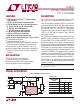
INRUSH AND POWERED ON
Once the PSE detects and optionally classifies the PD, the
PSE then powers on the PD. When the port voltage rises
above the V
HSON
threshold, it begins to source I
GPU
out of
the HSGATE pin. This current flows into an external capaci-
tor
(C
GATE
in Figure 3) that causes a voltage to ramp up the
gate of the external MOSFET. The external MOSFET acts as
a source follower and ramps the voltage up on the output
bulk capacitor (C
PORT
in Figure 3) thereby determining the
inrush current (I
INRUSH
in Figure 3).
To meet IEEE requirements, design I
INRUSH
to be approxi-
mately 100mA. See equation below:
I
INRUSH
= I
GPU
•
C
PORT
C
GATE
The LT4275 internal charge pump provides an N-channel
MOSFET solution, eliminating a larger and more costly
P-channel FET. The low R
DS(ON)
MOSFET also maximizes
LT4275A
HSGATE
GND
4275 F03
VPORT HSSRC
C
GATE
3.3k
+
C
PORT
VPORT
I
INRUSH
Figure 3. Programming I
INRUSH
power delivery and efficiency, reduces power and heat
dissipation, and eases thermal design.
The PWRGD pin is held low by its open drain output until
HSGATE charges up to approximately 7V above HSSRC.
The PWRGD pin is used to hold off the isolated power
supply until inrush is complete and the external MOSFET
is fully enhanced. The HSGATE pin will remain high and
the PWRGD pin pulled down until the port voltage falls
below V
HSOFF
or the AUX pin is above V
AUXT
.
AUXILIARY SUPPLY OVERRIDE
If the AUX pin is held above V
AUXT
, the LT4275 enters
auxiliary power supply override mode. In this mode
the signature resistor is disconnected, classification is
disabled, HSGATE is pulled down, and the PWRGD pin is
allowed to float. The T2P pin pulls down on the LT4275A/
LT4275B when no R
CLS
++
resistor is present. The T2P pin
alternates between pulling down and floating at f
T2P
on the
LT4275A when the R
CLS
++
resistor is present.