
Datasheet


LT4320/LT4320-1
5
4320fb
For more information www.linear.com/LT4320
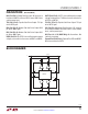
pin Functions
(DFN, PDIP/MSOP)
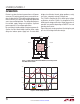
IN2 (Pin 1/Pin 1): Bridge Rectifier Input. IN2 connects to
the external NMOS transistors MTG2 source, MBG1 drain
and the power input.
TG2 (Pin 2/Pin 2): Topside Gate Driver Output. TG2 pin
drives MTG2 gate.
BG2 (Pin 3/Pin 5): Bottom-Side Gate Driver Output. BG2
pin drives MBG2 gate.
BG1 (Pin 4/Pin 6): Bottom-Side Gate Driver Output. BG1
pin drives MBG1 gate.
OUTN (Pin 5/Pin 7): OUTN is the rectified negative output
voltage, and connects to the sources of MBG1 and MBG2.
OUTP (Pin 6/Pin 9): OUTP is the rectified positive output
voltage that powers the LT4320 and connects to the drains
of MTG1 and MTG2.
TG1 (Pin 7/Pin 11): Topside Gate Driver Output. TG1 pin
drives MTG1 gate.
IN1 (Pin 8/Pin 12): Bridge Rectifier Input. IN1 connects
to the external NMOS transistors MTG1 source, MBG2
drain, and the power input.
NC (Pins 3, 4, 8, 10, MSOP Only): No Connections. Not
internally connected.
Exposed Pad (Pin 9/Pin 13): Exposed Pad, DFN and MSOP.
Must be connected to OUTN.
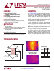
OUTP
LT4320 BD
MTG1
OUTN
BG1
IN1
LT4320
IN2
MBG1
BG2
MTG2
MBG2
TG1
+
–
~
~
TG2
CONTROL
block DiagraM