
Datasheet


LT4356-1/LT4356-2
14
4356fb
For more information www.linear.com/LT4356-1
ApplicAtions inForMAtion
MOSFET stress is the result of power dissipated within
the device. For long duration surges of 100ms or more,
stress is increasingly dominated by heat transfer; this is
a matter of device packaging and mounting, and heatsink
thermal mass. This is analyzed by simulation, using the
MOSFET thermal model.
For short duration transients of less than 100ms, MOSFET
survival is increasingly a matter of safe operating area
(SOA), an intrinsic property of the MOSFET. SOA quanti
-
fies the time required at any given condition of V
DS
and
I
D
to raise the junction temperature of the MOSFET to its
rated maximum. MOSFET SOA is expressed in units of
watt-squared-seconds (P
2
t). This figure is essentially con-
stant for intervals of less than 100ms for any given device
type, and rises to infinity under DC operating conditions.
Destruction mechanisms other than bulk die temperature
distort the lines of an accurately drawn SOA graph so that
P
2
t is not the same for all combinations of I
D
and V
DS
.
In particular P
2
t tends to degrade as V
DS
approaches the
maximum rating, rendering some devices useless for
absorbing energy above a certain voltage.
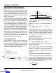
Calculating Transient Stress
To select a MOSFET suitable for any given application, the
SOA stress must be calculated for each input transient
which shall not interrupt operation. It is then a simple matter
to chose a device which has adequate SOA to survive the
maximum calculated stress. P
2
t for a prototypical transient
waveform is calculated as follows (Figure 4).
Let
a = V
REG
– V
IN
b = V
PK
– V
IN
(V
IN
= Nominal Input Voltage)
Then
P
2
t = I
LOAD
2
1
3
tr
b − a
(
)
3
b
+
1
2
t 2a
2
ln
b
a
+ 3a
2
+b
2
− 4ab
Typically V
REG
≈ V
IN
and t >> t
r
simplifying the above to
P
2
t =
1
2
I
LOAD
2
V
PK
– V
REG
( )
2
t (W
2
s)
For the transient conditions of V
PK
= 80V, V
IN
= 12V, V
REG
= 16V, t
r
= 10µs and t = 1ms, and a load current of 3A,
P
2
t is 18.4W
2
s—easily handled by a MOSFET in a D-pak
package. The P
2
t of other transient waveshapes is evaluated
by integrating the square of MOSFET power versus time.
Calculating Short-Circuit Stress
SOA stress must also be calculated for short-circuit condi
-
tions. Short-circuit P
2
t is given by:
P
2
t = (V
IN
• ΔV
SNS
/R
SNS
)
2
• t
TMR
(W
2
s)
where, ΔV
SNS
is the SENSE pin threshold, and t
TMR
is the
overcurrent timer interval.
For V
IN
= 14.7V, V
SNS
= 50mV, R
SNS
= 12mΩ and C
TMR
= 100nF, P
2
t is 6.6W
2
s—less than the transient SOA
calculated in the previous example. Nevertheless, to
account for circuit tolerances this figure should be doubled
to 13.2W
2
s.
Limiting Inrush Current and GATE Pin Compensation
The LT4356 limits the inrush current to any load capacitance
by controlling the GATE pin voltage slew rate. An external
capacitor can be connected from GATE to ground to slow
down the inrush current further at the expense of slower
turn-off time. The gate capacitor is set at:
C1 =
I
I
GATE(UP)
INRUSH
•C
L
Figure 4. Safe Operating Area Required to Survive Prototypical
Transient Waveform
V
PK
τ
V
IN
4356 F04
V
REG
t
r
Downloaded from Arrow.com.Downloaded from Arrow.com.Downloaded from Arrow.com.Downloaded from Arrow.com.Downloaded from Arrow.com.Downloaded from Arrow.com.Downloaded from Arrow.com.Downloaded from Arrow.com.Downloaded from Arrow.com.Downloaded from Arrow.com.Downloaded from Arrow.com.Downloaded from Arrow.com.Downloaded from Arrow.com.Downloaded from Arrow.com.