
Datasheet


LT4363
12
4363fa
t
FLT
= 15.5ms/µF
TOTAL FAULT TIMER = t
FLT
+ t
WARNING
t
WARNING
= 16.67ms/µF
t
FLT
= 96.9ms/µF t
WARNING
= 16.67ms/µF
V
TMR(V)
I
TMR
= 6µA I
TMR
= 6µA
V
DS
= 75V
(I
TMR
= 50µA)
V
DS
= 10V
(I
TMR
= 8µA)
1.375
1.275
TIME
4363 F01
0.50
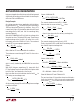
Fault Timer Operation in Overcurrent
TMR pin behavior in overcurrent is substantially the same
as in overvoltage. In the presence of an overcurrent con-
dition when the LT4363 regulates the output current, the
timer charges from 0.5V to 1.275V with a current that
varies as a function of V
DS
(see Figure 2). The current is
about 5 times the value produced in overvoltage, under
similar conditions V
DS
, increasing linearly from 8µA with
V
DS
< 0.5V to 260µA with V
DS
= 80V. V
DS
is inferred from
the drop across V
CC
and OUT. Because V
DS
is measured
indirectly, clamping or filtering at the V
CC
pin affects the
timer current response. A graph of Overcurrent TMR Cur-
rent vs (V
CC
– V
OUT
) is shown in the Typical Performance
Characteristics.
When TMR reaches 1.275V, the F LT pin is latched low as
an early warning of impending shutdown. But unlike the
overvoltage case, the timer current is not reduced and
instead continues unabated until TMR reaches 1.375V,
producing an early warning period given by:
C
TMR
= t
WARNING
•
I
TMR
100mV
When TMR reaches 1.375V, the MOSFET is turned off and
allowed to cool for an extended period. The total elapsed
time between the onset of current limiting and turn-off
is given by:
t
LIM
= C
TMR
•
0.875V
I
TMR
Because I
TMR
is a function of V
CC
– V
OUT
, the exact time
in current limit depends upon the input waveform and the
time required for the output current to come into regulation.
Cool Down Phase
Cool Down behavior is the same whether initiated by
overvoltage or overcurrent. During the cool down phase,
the timer continues to charge from 1.375V to 4.3V with
2µA, and then discharges back down to 0.5V with 2µA,
for a total equivalent voltage swing of 6.725V. The cool
down time is given by:
t
COOL
= C
TMR
•
2.925V + 3.8V
2µA
Up to this point the operation of the LT4363-1 and LT4363-2
is the same. Behavior at the end of the cool down phase
and in response to the SHDN pin is entirely different.
At the end of the cool down phase the LT4363-1 remains
latched off and F LT remains low. It may be restarted by
pulling the SHDN pin low for at least 100µs or by cycling
power. The cool down phase may be interrupted at any-
time by pulling SHDN low for at least 1s/µF of C
TMR
; the
LT4363-1 will restart when SHDN goes high.
The LT4363-2 will automatically retry at the end of the
cool down phase. Retry is inhibited if the OV pin is above
1.275V; this prevents repetitive retries while the input is
held in a sustained overvoltage condition. Retry is auto-
APPLICATIONS INFORMATION
Figure 1. Overvoltage Fault Timer Current
Figure 2. Overcurrent Fault Timer Current
t
FLT
= 2.98ms/µF
TOTAL FAULT TIMER = t
FLT
+ t
WARNING
t
FLT
= 22.14ms/µF
t
WARNING
= 2.86ms/µF
t
WARNING
= 0.38ms/µF
V
TMR(V)
V
DS
= 10V
(I
TMR
= 35µA)
1.375
1.275
0.50
TIME
4363 F02
V
DS
= 80V
(I
TMR
= 260µA)