
Datasheet


LT4363
13
4363fa
APPLICATIONS INFORMATION
matically initiated once the OV pin falls below 1.268V. OV
has no effect on initial start-up when power is first applied
and upon exiting shutdown. The cool down phase may
be interrupted in the LT4363-2 by pulling SHDN low for
at least 1s/µF of C
TMR
.
For both the LT4363-1 and LT4363-2 the F LT pin goes
high in shutdown and is cleared high when power is first
applied to V
CC
. If F LT is set low, it can be reset during the
cool down phase by pulling SHDN low for at least 1s/µF
of C
TMR
.
Intermittent Fault Conditions
Brief overvoltage or overcurrent conditions interrupt the
operation of the timer. If the TMR pin has not yet reached
1.275V when the input falls below the regulation value
or drops out of current limit, the timer capacitor is dis-
charged back to 0.5V with a 2µA current sink. If the TMR
voltage crosses 1.275V F LT is set low. If the overvoltage
or overcurrent abates before reaching 1.375V, the timer
capacitor discharges with 2µA back to 0.5V, whereupon
F LT resets high. If several short overvoltage or overcurrent
events occur in rapid succession, the timer capacitor will
integrate the charging and discharging currents.
MOSFET Selection
The LT4363 drives an N-channel MOSFET to conduct the
load current. The important features of the MOSFET are
on-resistance R
DS(ON)
, the maximum drain-source voltage
V
(BR)DSS
, the threshold voltage, and the SOA.
The maximum allowable drain-source voltage must be
higher than the supply voltage. If the output is shorted
to ground or during an overvoltage event, the full supply
voltage will appear across the MOSFET.
The gate drive for the MOSFET is guaranteed to be more
than 10V and less than 16V for those applications with V
CC
higher than 9V. This allows the use of standard threshold
voltage N-channel MOSFETs. For systems with V
CC
less
than 9V, a logic level MOSFET is required since the gate
drive can be as low as 4.5V.
The SOA of the MOSFET must encompass all fault condi-
tions. In normal operation the pass transistor is fully on,
dissipating very little power. But during either overvoltage
or overcurrent faults, the GATE pin is controlled to regu-
late either the output voltage or the current through the
MOSFET. Large current and high voltage drop across the
MOSFET can coexist in these cases. The SOA curves of
the MOSFET must be considered carefully along with the
selection of the fault timer capacitor.
Transient Stress in the MOSFET
During an overvoltage event, the LT4363 drives a series
pass MOSFET to regulate the output voltage at an acceptable
level. The load circuitry may continue operating throughout
this interval, but only at the expense of dissipation in the
MOSFET pass device. MOSFET dissipation or stress is a
function of the input voltage waveform, regulation voltage
and load current. The MOSFET must be sized to survive
this stress.
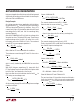
Most transient event specifications use the prototypi-
cal waveshape shown in Figure 3, comprising a linear
ramp of rise time t
r
, reaching a peak voltage of V
PK
and
exponentially decaying back to V
IN
with a time constant
of τ. A common automotive transient specification has
constants of t
r
= 10µs, V
PK
= 80V and τ = 1ms. A surge
condition known as load dump commonly has constants
of t
r
= 5ms, V
PK
= 60V and τ = 200ms.
MOSFET stress is the result of power dissipated within
the device. For long duration surges of 100ms or more,
stress is increasingly dominated by heat transfer; this is
a matter of device packaging and mounting, and heat sink
thermal mass. This is best analyzed by simulation, using
the MOSFET thermal model.
For short duration transients of less than 100ms, MOSFET
survival is increasingly a matter of safe operating area
Figure 3. Prototypical Transient Waveform
V
PK
τ
V
IN
4363 F03
t
r