
Datasheet


LT4363
14
4363fa
(SOA), an intrinsic property of the MOSFET. SOA quanti-
fies the time required at any given condition of V
DS
and
I
D
to raise the junction temperature of the MOSFET to its
rated maximum. MOSFET SOA is expressed in units of
watt-squared-seconds (P
2
t). This figure is essentially con-
stant for intervals of less than 100ms for any given device
type, and rises to infinity under DC operating conditions.
Destruction mechanisms other than bulk die temperature
distort the lines of an accurately drawn SOA graph so that
P
2
t is not the same for all combinations of I
D
and V
DS
.
In particular P
2
t tends to degrade as V
DS
approaches the
maximum rating, rendering some devices useless for
absorbing energy above a certain voltage.
When a fast input voltage step occurs, the current through
the pass transistor to supply the load and charge up the out-
put capacitor can be high enough to trigger an overcurrent
event. The gate pulls low to 1V above the OUT pin, turning
off the MOSFET momentarily. The internal charge pump
will then start to pull the GATE pin high and turn on the
MOSFET to support the load current and charge up the
OUT pin. The fault timer may not start yet because the
current level is below the overcurrent limit threshold and
the output voltage has not reached the servo voltage. This
extra stress needs to be included in calculating the overall
stress level of the MOSFET.
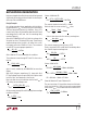
Calculating Transient Stress
To select a MOSFET suitable for any given application, the
SOA stress must be calculated for each input transient
which shall not interrupt operation. It is then a simple matter
to choose a device which has adequate SOA to survive the
maximum calculated stress. P
2
t for a prototypical transient
waveform is calculated as follows (Figure 4):
Let
a = V
REG
– V
IN
b = V
PK
– V
IN
(V
IN
= Nominal Input Voltage)
Then
P
2
t = I
LOAD
2
•
1
3
t
r
b– a
( )
3
b
+
1
2
τ 2a
2
ln
b
a
+ 3a
2
+b
2
− 4ab
Typically V
REG
≈ V
IN
and τ » t
r
simplifying the above to
P
2
t =
1
2
I
LOAD
2
V
PK
– V
REG
( )
2
τ [W
2
s]
For the transient conditions of V
PK
= 80V, V
IN
= 12V,
V
REG
= 16V, t
r
= 10µs and τ = 1ms, and a load current
of 3A, P
2
t is 18.4W
2
s – easily handled by a MOSFET in
a DPAK package. The P
2
t of other transient waveshapes
is evaluated by integrating the square of MOSFET power
over time. LTSpice can be used to simulate timer behavior
for more complex transients and cases where overvoltage
and overcurrent faults coexist.
Calculating Short-Circuit Stress
SOA stress must also be calculated for short-circuit condi-
tions. Short-circuit P
2
t is given by:
P
2
t = ΔV
DS
•
ΔV
SNS
R
SNS
2
• t
TMR
[W
2
s]
Where ∆V
DS
is the voltage across the MOSFET, and ∆V
SNS
is the SNS pin threshold, and t
TMR
is the overcurrent timer
interval.
For V
IN
= 15V, ∆V
DS
= 13V (V
OUT
= 2V), ∆V
SNS
= 50mV,
R
SNS
= 12mΩ and C
TMR
= 100nF, P
2
t is 6.3W
2
s – less
than the transient SOA calculated in the previous example.
Nevertheless, to account for circuit tolerances this figure
should be doubled to 12.6W
2
s.
APPLICATIONS INFORMATION
Figure 4. Safe Operating Area Required to Survive Prototypical
Transient Waveform
V
PK
τ
V
IN
4363 F04
V
REG
t
r