
Datasheet


LT4363
15
4363fa
C
TMR
0.1µF
R
SNS
10mΩ
Q1
IRLR2908
Q2
IRLR2908
V
IN
12V
V
OUT
12V, 3A
CLAMPED
AT 16V
4363 F06
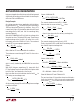
LT4363DE-2
GND TMR
9 12
OUT
2
SNS
3
SHDN
6
UV
8
OV
7
V
CC
5
FLT
ENOUT
FB
10
11
1
C1
47nF
D1*
SMAJ58CA
R2
4.99k
R1
57.6k
GATE
4
R7
10k
R5
1M
Q3
2N3904
D2
1N4148
R3
10Ω
R4
10Ω
*DIODES INC.
APPLICATIONS INFORMATION
Figure 6. Overvoltage Regulator with N-channel MOSFET
Reverse Input Protection
Figure 5. External GATE network
Limiting Inrush Current and GATE Pin Compensation
The LT4363 limits the inrush current to any load capacitance
by controlling the GATE pin voltage slew rate. An external
capacitor can be connected from GATE to ground to reduce
the inrush current at the expense of slower turn-off time.
The gate capacitor is set at:
C1=
I
GATE(UP)
I
INRUSH
• C
L
The LT4363 does not need extra compensation compo-
nents at the GATE pin for stability during an overvoltage or
overcurrent event. With transient input voltage slew rates
faster than 5V/µs, a gate capacitor, C1, to ground is needed
to prevent self enhancement of the N-channel MOSFET.
The extra gate capacitance slows down the turn off time
during fault conditions and may allow excessive current
during an output short event. An extra resistor, R1, in series
with the gate capacitor can improve the turn off time. A
diode, D1, should be placed across R1 with the cathode
connected to C1 as shown in Figure 5.
threshold during a fault. The pass transistor is not allowed
to turn back on even after the cool down period has finished.
This prevents the pass transistor from cycling between ON
and OFF states when the input voltage stays at an elevated
level for a long period of time, reducing the stress on the
N-channel MOSFET. For the latch-off version, LT4363-1,
the overvoltage comparator function is not available.
Reverse Input Protection
A blocking diode is commonly employed to protect the
load when reverse input is possible, such as in automo-
tive applications. This diode causes extra power loss,
generates heat, and reduces the available supply voltage
range. During cold crank, the extra voltage drop across
the diode is particularly undesirable.
The LT4363 is designed to withstand reverse voltage with-
out damage to itself. The V
CC
, SHDN, UV, and OV pins can
withstand up to 60V of DC voltage below the GND potential.
Back-to-back MOSFETs must be used to block the current
path through Q1’s body diode (Figure 6). Figure 7 shows
the approach with a P-channel MOSFET in place of Q2.
C1
R3
4363 F05
LT4363
GATE
Q1
R1
D1
IN4148W
Undervoltage/Overvoltage Comparators
The LT4363 has both undervoltage and overvoltage com-
parators that can be used to sense the input supply volt-
age. When the voltage at the UV pin is below the 1.275V
threshold, the GATE pin is held low to keep the external
MOSFET off. The supply voltage at the V
CC
pin should be
at least 4V for the UV comparator to function.
The overvoltage comparator prevents the LT4363-2 from
restarting if the voltage at the OV pin is above the 1.275V