
Datasheet
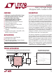


LT4363
4
4363fa
Note 2: All currents into device pins are positive all current out of device
pins are negative. All voltages are referenced to GND unless otherwise
specified.
Note 3: An internal clamp limits the GATE pin to a minimum of 10V above
the OUT pin. Driving this pin to voltages beyond the clamp may damage
the device.
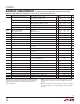
SYMBOL PARAMETER CONDITIONS MIN TYP MAX UNITS
I
TMR
TMR Pull-up Current, Overvoltage
TMR = 1V, FB = 1.5V, ΔV
DS
= 0.5V
TMR = 1V, FB = 1.5V, ΔV
DS
= 75V
l
l
–1.7
–42
–4
–50
–6
–58
µA
µA
TMR Pull-up Current, OV Warning
TMR = 1.325V, FB = 1.5V, ΔV
DS
= 0.5V
l
–3 –5 –7 µA
TMR Pull-up Current, Overcurrent
TMR = 1V, ΔV
SNS
= 100mV, ΔV
DS
= 0.5V
TMR = 1V, ΔV
SNS
= 100mV, ΔV
DS
= 80V
l
l
–5
–190
–9
–250
–13
–310
µA
µA
TMR Pull-up Current, Cool Down
TMR = 3V, FB = 1.5V, ΔV
SNS
= 0V, ΔV
DS
= 0V
l
–1 –2.3 –3.5 µA
TMR Pin Pull-down Current, Cool Down
V
TMR
= 3V, FB = 1.5V, ΔV
SNS
= 0V, ΔV
DS
= 0V
l
1 2 4 µA
V
TMR(F)
V
TMR(G)
V
TMR(R)
TMR Fault Threshold
TMR Gate Off Threshold
TMR Restart Threshold
TMR Rising
TMR Rising
TMR Falling, LT4363-2
l
l
l
1.235
1.335
0.47
1.275
1.375
0.5
1.31
1.41
0.53
V
V
V
ΔV
TMR
Early Warning Window V
TMR(G) –
V
TMR(F)
l
80 100 120 mV
V
TMR(H)
TMR Cool Down High Threshold V
CC
= 7V to 80V, TMR Rising
l
3.7 4.3 5 V
V
UV
UV Input Threshold UV Rising
l
1.24 1.275 1.31 V
V
UV(HYST)
UV Input Hysteresis 12 mV
V
OV
OV Input Threshold OV Rising
l
1.24 1.275 1.31 V
V
OV(HYST)
OV Input Hysteresis 7.5 mV
I
IN
UV, OV Input Current UV = 1.275V
UV = –60V
l
l
±0.2
–1
±1
–2
µA
mA
I
LEAK
F LT , ENOUT Leakage Current F LT , ENOUT = 80V
l
±0.5 ±2.5 µA
V
OL
F LT , ENOUT Output Low I
SINK
= 0.1mA
I
SINK
= 2mA
l
l
300
2
800
9
mV
V
ΔV
OUT(TH)
OUT High Threshold
ΔV
OUT
= V
CC
– V
OUT
, ENOUT From Low to High
l
0.25 0.5 0.75 V
ΔV
OUT(RST)
OUT Reset Threshold ENOUT From High to Low
l
1.9 2.7 3.6 V
I
OUT
OUT Input Current V
CC
= OUT = 12V, SHDN Open
V
CC
= OUT = 12V, SHDN = 0V
l
l
0.25
0.25
0.5
1
mA
mA
V
SHDN
SHDN Threshold V
CC
= 4V to 80V
l
0.6
0.4
1.4 1.7
2.1
V
V
V
SHDN(Z)
SHDN Open Voltage V
CC
= 4V to 80V
l
2.2 V
I
SHDN
SHDN Current SHDN = 0.4V
l
–1 –4 –8 µA
t
RESET
SHDN Reset Time SHDN ≤ 0.4V; LT4363-1
l
100 µs
D Retry Duty Cycle; Overvoltage V
CC
= 80V, OUT = 16V, FB = 1.5V; LT4363-2
l
1 2 %
Retry Duty Cycle; Output Short V
CC
= 12V, OUT = 0V, ∆V
SNS
= 100mV; LT4363-2
l
0.76 1 %
t
OFF(UV)
Undervoltage Turn Off Propagation Delay UV Steps from 1.5V to 1V
l
2 5 µs
t
OFF(OV)
Overvoltage Turn Off Propagation Delay FB Steps from 0V to 1.5V; OUT = 0V
l
0.25 1 µs
t
OFF(OC)
Overcurrent Turn Off Propagation Delay ∆V
SNS
Steps from 0V to 150mV; OUT = 0V
l
1 2.5 µs
Note 1: Stresses beyond those listed under Absolute Maximum Ratings
may cause permanent damage to the device. Exposure to any Absolute
Maximum Rating condition for extended periods may affect device
reliability and lifetime.
ELECTRICAL CHARACTERISTICS
The l denotes the specifications which apply over the full operating
temperature range, otherwise specifications are at T
A
= 25°C. V
CC
= 12V, unless otherwise noted.