
Datasheet


LT6013/LT6014
13
60134fb
APPLICATIO S I FOR ATIO
WUUU
Preserving Input Precision
Preserving the input accuracy of the
LT6013 and
LT6014
requires that the applications circuit and PC board layout
do not introduce errors comparable to or greater than the
10µV typical offset of the amplifiers. Temperature differen-
tials across the input connections can generate thermo-
couple voltages of 10’s of microvolts so the connections
to the input leads should be short, close together and away
from heat dissipating components. Air currents across the
board can also generate temperature differentials.
The extremely low input bias currents allow high accuracy
to be maintained with high impedance sources and feed-
back resistors. The LT6013 and LT6014 low input bias cur-
rents are obtained by a cancellation circuit on-chip. This
causes the resulting I
B
+
and I
B
–
to be uncorrelated, as
implied by the I
OS
specification being comparable to I
B
. Do
not try to balance the input resistances in each input lead;
instead keep the resistance at either input as low as pos-
sible for maximum accuracy.
Leakage currents on the PC board can be higher than the
input bias current. For example, 10GΩ of leakage between
a 15V supply lead and an input lead will generate 1.5nA!
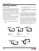
Surround the input leads with a guard ring driven to the
same potential as the input common mode to avoid exces-
sive leakage in high impedance applications.
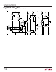
Input Protection
The LT6013/LT6014 features on-chip back-to-back diodes
between the input devices, along with 500Ω resistors in
series with either input. This internal protection limits the
input current to approximately 10mA (the maximum al-
lowed) for a 10V differential input voltage. Use additional
external series resistors to limit the input current to 10mA
in applications where differential inputs of more than 10V
are expected. For example, a 1k resistor in series with each
input provides protection against 30V differential voltage.
Input Common Mode Range
The LT6013/LT6014 output is able to swing close to each
power supply rail (rail-to-rail out), but the input stage is
limited to operating between V
–
+ 1V and V
+
– 1.2V. Exceed-
ing this common mode range will cause the gain to drop
to zero; however, no phase reversal will occur.
Total Input Noise
The LT6013 and LT6014 amplifiers contribute negligible
noise to the system when driven by sensors (sources) with
impedance between 10kΩ and 1MΩ. Throughout this
range, total input noise is dominated by the 4kTR
S
noise
of the source. If the source impedance is less than 10kΩ,
the input voltage noise of the amplifier starts to contribute
with a minimum noise of 9.5nV/√Hz for very low source im-
pedance. If the source impedance is more than 1MΩ, the
input current noise of the amplifier, multiplied by this high
impedance, starts to contribute and eventually dominate.
Total input noise spectral density can be calculated as:
v e kTR i R
n TOTAL n S n S()
()=+ +
2
2
4
where e
n
= 9.5nV/√Hz , i
n
= 0.15pA/√Hz and R
S
is the total
impedance at the input, including the source impedance.
Capacitive Loads
The LT6013 and LT6014 can drive capacitive loads up to
500pF at a gain of 5. The capacitive load driving capability
increases as the amplifier is used in higher gain configu-
rations. A small series resistance between the output and
the load further increases the amount of capacitance that
the amplifier can drive.