
Datasheet


LT6220/LT6221/LT6222
1
622012fb
For more information www.linear.com/LT6220/LT6221/LT6222
Typical applicaTion
Single/Dual/Quad 60MHz,
20V/µs, Low Power, Rail-to-Rail Input
and Output Precision Op Amps
The LT
®
6220/LT6221/LT6222 are single/dual/quad, low
power, high speed rail-to-rail input and output operational
amplifiers with excellent DC performance. The LT6220/
LT6221/LT6222 feature reduced supply current, lower
input offset voltage, lower input bias current and higher
DC gain than other devices with comparable bandwidth.
Typically, the LT6220/LT6221/LT6222 have an input offset
voltage of less than 100µV, an input bias current of less than
15nA and an open-loop gain of 100V/mV. The parts have
an input range that includes both supply rails and an output
that swings within 10mV of either supply rail to maximize
the signal dynamic range in low supply applications.
The LT6220/LT6221/LT6222 maintain performance for
supplies from 2.2V to 12.6V and are specified at 3V, 5V
and ±5V supplies. The inputs can be driven beyond the
supplies without damage or phase reversal of the output.
The LT6220 is housed in the 8-lead SO package with the
standard op amp pinout as well as the 5-lead SOT-23
package. The LT6221 is available in 8-lead SO and DFN
(3mm × 3mm low
profile dual fine pitch leadless) packages
with the standard op amp pinout. The LT6222 features the
standard quad op amp configuration and is available in
the 16-lead SSOP package. The LT6220/LT6221/LT6222
can be used as plug-in replacements for many op amps
to improve input/output range and performance.
applicaTions
n
Gain Bandwidth Product: 60MHz
n
Input Common Mode Range Includes Both Rails
n
Output Swings Rail-to-Rail
n
Low Quiescent Current: 1mA Max
n
Input Offset Voltage: 350µV Max
n
Input Bias Current: 150nA Max
n
Wide Supply Range: 2.2V to 12.6V
n
Large Output Current: 50mA Typ
n
Low Voltage Noise: 10nV√Hz Typ
n
Slew Rate: 20V/µs Typ
n
Common Mode Rejection: 102dB Typ
n
Power Supply Rejection: 105dB Typ
n
Open-Loop Gain: 100V/mV Typ
n
Operating Temperature Range: –40°C to 85°C
n
Single in the 8-Lead SO and 5-Lead Low Profile
(1mm) ThinSOT™ Packages
n
Dual in the 8-Lead SO and (3mm × 3mm) DFN
Packages
n
Quad in the 16-Lead SSOP Package
n
Low Voltage, High Frequency Signal Processing
n
Driving A/D Converters
n
Rail-to-Rail Buffer Amplifiers
n
Active Filters
n
Video Amplifiers
n
Fast Current Sensing Amplifiers
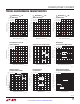
Stepped-Gain Photodiode Amplifier
V
OS
Distribution, V
CM
= 0V
(S8, PNP Stage)
–
+
I
PD
PHOTODIODE
~4pF
V
S
+
V
S
+
V
S
+
V
S
–
V
S
–
LT6220
100k
3.24k
33k
10k
1pF
30pF
LT1634-1.25
V
OUT
V
S
= ±1.5V TO ±5V
V
OUT
= 0V TO –1.25V, TRANSIMPEDANCE = 100k
V
OUT
<
–1.25V, TRANSIMPEDANCE = (100k || 3.24k) = 3.14k
622012 TA01a
INPUT OFFSET VOLTAGE (µV)
–250
PERCENT OF UNITS (%)
30
40
50
150
622012 TA01b
20
10
25
35
45
15
5
0
–150
–50 0
50
250
V
S
= 5V, 0V
V
CM
= 0V
L, LT, LTC , LT M, Linear Technology and the Linear logo are registered trademarks and
ThinSOT is a trademark of Linear Technology Corporation. All other trademarks are the property
of their respective owners.
FeaTures DescripTion