
Datasheet


LT6552
12
6552f
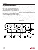
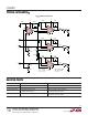
Figure 5. Simplified Schematic
6
7
4
Q2
Q3
Q4
Q5
Q6
Q1
Q7
Q8
Q10
Q11
Q12
Q13
Q14
Q20Q19
Q9
Q15
Q16
R1
R5 R6
R3 R4
R2
COMPLEMENTARY
DRIVE GENERATOR
Q21
Q22
V
+
V
+
V
–
V
–
OUT
CM
DESD10
DESD9
5
V
+
V
+
V
–
SHDN
DESD12
DESD11
V
+
V
–
DESD2
DESD1
V
+
V
–
DESD4
DESD3
V
+
V
–
DESD8
DESD7
V
+
V
–
DESD6
DESD5
R
IN1
R
IN2
R
IN3
R
IN4
+IN
3
–IN
2
REF
1
FB
8
I6
I5
I4I3I2I1
Q18Q17
6552 FO5
BIAS
Amplifier Characteristics
Figure 5 shows a simplified schematic of the LT6552.
There are two input stages; the first one consists of
transistors Q1 to Q8 for the (+) and (–) inputs while the
second input stage consists of transistors Q9 to Q16 for
the reference and feedback inputs. This topology provides
high slew rates at low supply voltages. The input common
mode range extends from ground to typically 1.75V from
V
CC
, and is limited by 2V
BE
’s plus a saturation voltage of
current sources I1-I4. Each input stage drives the degen-
eration resistors of PNP and NPN current mirrors, Q17 to
Q20, that convert the differential signals into a single-
ended output. The complementary drive generator sup-
plies current to the output transistors that swing from rail-
to-rail.
The current generated through R1 or R2, divided by the
capacitor CM, determines the slew rate. Note that this
current, and hence the slew rate, are proportional to the
magnitude of the input step. The input step equals the
output step divided by the closed-loop gain. The highest
slew rates are therefore obtained in the lowest gain con-
figurations. The Typical Performance Characteristic Curve
of Slew Rate vs Closed-Loop Gain shows the details.
ESD
The LT6552 has reverse-biased ESD protection diodes on
all inputs and outputs, as shown in Figure 5. If these pins
are forced beyond either supply, unlimited current will
flow through these diodes. If the current is transient in
nature and limited to 100mA or less, no damage to the
device will occur.
APPLICATIO S I FOR ATIO
WUUU