
Datasheet


LT6552
14
6552f
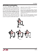
SHDN Pin
The LT6552 includes a shutdown feature that disables the
part, reducing quiescent current and making the output
high impedance. The part can be shutdown by bringing the
SHDN pin within 0.5V of V
–
. When shutdown the supply
current is typically 400µA and the output leakage current
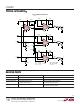
DD Package
8-Lead Plastic DFN (3mm × 3mm)
(Reference LTC DWG # 05-08-1698)
is 0.25µA (V
–
≤ V
OUT
≤ V
+
). In normal operation the SHDN
can be tied to V
+
or left floating; if the pin is left uncon-
nected, an internal FET pull-up will keep the LT6552 fully
operational.
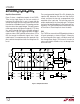
APPLICATIO S I FOR ATIO
WUUU
U
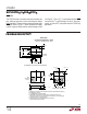
PACKAGE DESCRIPTIO
3.00 ±0.10
(4 SIDES)
NOTE:
1. DRAWING TO BE MADE A JEDEC PACKAGE OUTLINE M0-229 VARIATION OF (WEED-1)
2. DRAWING NOT TO SCALE
3. ALL DIMENSIONS ARE IN MILLIMETERS
4. DIMENSIONS OF EXPOSED PAD ON BOTTOM OF PACKAGE DO NOT INCLUDE
MOLD FLASH. MOLD FLASH, IF PRESENT, SHALL NOT EXCEED 0.15mm ON ANY SIDE
5. EXPOSED PAD SHALL BE SOLDER PLATED
6. SHADED AREA IS ONLY A REFERENCE FOR PIN 1 LOCATION
ON TOP AND BOTTOM OF PACKAGE
0.38 ± 0.10
BOTTOM VIEW—EXPOSED PAD
1.65 ± 0.10
(2 SIDES)
0.75 ±0.05
R = 0.115
TYP
2.38 ±0.10
(2 SIDES)
14
85
PIN 1
TOP MARK
(NOTE 6)
0.200 REF
0.00 – 0.05
(DD8) DFN 1203
0.25 ± 0.05
2.38 ±0.05
(2 SIDES)
RECOMMENDED SOLDER PAD PITCH AND DIMENSIONS
1.65 ±0.05
(2 SIDES)2.15 ±0.05
0.50
BSC
0.675 ±0.05
3.5 ±0.05
PACKAGE
OUTLINE
0.25 ± 0.05
0.50 BSC