
Datasheet


LT6555
11
6555f
APPLICATIO S I FOR ATIO
WUUU
This systematic gain error can be significantly reduced by
lowering the value of the 75Ω series termination resistors.
The compromise of this approach is an increased depen-
dence on the accuracy of the 75Ω shunt termination at the
receiving end of the line. A table of values for 1% series
termination resistors from n = 2 to n = 4 is shown below.
NUMBER OF DEVICES (n) SERIES R
T
2 63.9
3 56.2
4 49.9
Another approach that does not compromise gain accu-
racy is to connect the outputs directly together before the
series termination. In this case, there will be slightly
increased output glitching and supply current spiking
during the EN pin switching, but the additional output
loading will not increase the gain error, and the series
termination resistors remain at their ideal value for AC
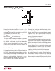
response. See Figure 4 for a scope photo showing the
result of the outputs connected both before and after the
series terminations, and Figure 8 for a full schematic of a
4:1 RGB multiplexer with the output pins directly con-
nected together. It is imperative that the output traces be
as short as possible before the series termination in order
to reduce capacitance and minimize AC peaking.
Figure 4. 4-Input Router Switching with Outputs Directly
Connected and with Outputs Connected After 63.9Ω
Series Termination
ESD Protection
The LT6555 has reverse-biased ESD protection diodes on
all pins. If any pins are forced a diode drop above the
positive supply or a diode drop below the negative supply,
large currents may flow through these diodes. If the
current is kept below 10mA, no damage to the devices will
occur.
TIME (µs)
0
MULTIPLEXED OUTPUT (V)
SUPPLY CURRENT (mA)
–0.5
0
0.5
4
6555 F04
–1.0
1
2
3
0.5
1.5
2.5
3.5
1.5
1.0
0
50
I
S
–
I
S
+
100
150
V
S
= ±5V
V
IN(AMP1)
= –0.5V
V
IN(AMP2)
= 0.5V
R
L
= 150Ω
OUTPUTS
DIRECTLY
CONNECTED
SERIES 63.9Ω
AT EACH OUTPUT
TYPICAL APPLICATIO
U
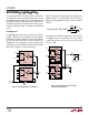
RGB Multiplexer Demo Board
The DC858A Demo Board illustrates optimal routing,
bypassing and termination using the LT6555 as an
RGB video multiplexer. The schematic is shown in Fig-
ure 5. All inputs and outputs are routed to have a charac-
teristic impedance of 75Ω and 75Ω input shunt and output
series terminations are connected as close to the part as
possible. The board is fabricated with four layers with
internal ground and power planes. For ideal operation, a
75Ω load termination should be connected at the output.
The LT6555’s gain of 2 will compensate for the resulting
divider between the series and load termination resistors.
Figures 6 and 7 show the topside and bottom side board
layout and placement.