
Datasheet


LT6555
15
6555f
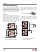
UF Package
24-Lead Plastic QFN (4mm × 4mm)
(Reference LTC DWG # 05-08-1697)
PACKAGE DESCRIPTIO
U
4.00 ± 0.10
(4 SIDES)
NOTE:
1. DRAWING PROPOSED TO BE MADE A JEDEC PACKAGE OUTLINE MO-220 VARIATION (WGGD-X)—TO BE APPROVED
2. DRAWING NOT TO SCALE
3. ALL DIMENSIONS ARE IN MILLIMETERS
4. DIMENSIONS OF EXPOSED PAD ON BOTTOM OF PACKAGE DO NOT INCLUDE
MOLD FLASH. MOLD FLASH, IF PRESENT, SHALL NOT EXCEED 0.15mm ON ANY SIDE, IF PRESENT
5. EXPOSED PAD SHALL BE SOLDER PLATED
6. SHADED AREA IS ONLY A REFERENCE FOR PIN 1 LOCATION
ON THE TOP AND BOTTOM OF PACKAGE
PIN 1
TOP MARK
(NOTE 6)
0.40 ± 0.10
2423
1
2
BOTTOM VIEW—EXPOSED PAD
2.45 ± 0.10
(4-SIDES)
0.75 ± 0.05
R = 0.115
TYP
0.25 ± 0.05
0.50 BSC
0.200 REF
0.00 – 0.05
(UF24) QFN 0105
RECOMMENDED SOLDER PAD PITCH AND DIMENSIONS
0.70 ±0.05
0.25 ±0.05
0.50 BSC
2.45 ± 0.05
(4 SIDES)
3.10 ± 0.05
4.50 ± 0.05
PACKAGE OUTLINE
PIN 1 NOTCH
R = 0.20 TYP OR
0.35 × 45° CHAMFER
Information furnished by Linear Technology Corporation is believed to be accurate and reliable.
However, no responsibility is assumed for its use. Linear Technology Corporation makes no represen-
tation that the interconnection of its circuits as described herein will not infringe on existing patent rights.