
Datasheet

LT6555
7
6555f
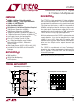
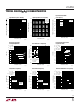
IN1A (Pin 1): Channel 1 Input A. This pin has a nominal
impedance of 400kΩ and does not have any internal
termination resistor.
DGND (Pin 2): Digital Ground Reference for Enable Pin.
This pin is normally connected to ground.
IN2A (Pin 3): Channel 2 Input A. This pin has a nominal
impedance of 400kΩ and does not have any internal
termination resistor.
V
REF
(Pin 4): Voltage Reference for Input Clamping. This
is the tap to an internal voltage divider that defines mid-
supply. It is normally connected to ground in dual supply,
DC coupled applications.
IN3A (Pin 5): Channel 3 Input A. This pin has a nominal
impedance of 400kΩ and does not have any internal
termination resistor.
AGND1 (Pin 6): Analog Ground for the 360Ω Gain Resis-
tor of Channel 1.
IN1B (Pin 7): Channel 1 Input B. This pin has a nominal
impedance of 400kΩ and does not have any internal
termination resistor.
AGND2 (Pin 8): Analog Ground for the 360Ω Gain Resis-
tor of Channel 2.
IN2B (Pin 9): Channel 2 Input B. This pin has a nominal
impedance of 400kΩ and does not have any internal
termination resistor.
AGND3 (Pin 10): Analog Ground for the 360Ω Gain
Resistor of Channel 3.
IN3B (Pin 11): Channel 3 Input B. This pin has a nominal
impedance of 400kΩ and does not have any internal
termination resistor.
V
–
(Pin 12): Negative Supply Voltage. V
–
pins are not in-
ternally connected to each other and must all be connected
externally. Proper supply bypassing is necessary for best
performance. See the Applications Information section.
V
+
(Pins 13, 14, 24): Positive Supply Voltage. V
+
pins are
not internally connected to each other and must all be
connected externally. Proper supply bypassing is neces-
sary for best performance. See the Applications Informa-
tion section.
V
–
(Pin 15): Negative Supply Voltage for Channel 3 Output
Stage. V
–
pins are not internally connected to each other
and must all be connected externally. Proper supply bypass-
ing is necessary for best performance. See the Applications
Information section.
OUT3 (Pin 16): Channel 3 Output. It is twice the selected
channel 3 input and performs optimally with a 150Ω load
(a double terminated 75Ω cable).
V
+
(Pin 17): Positive Supply Voltage for Channels 2 and 3
Output Stages. V
+
pins are not internally connected to each
other and must all be connected externally. Proper supply
bypassing is necessary for best performance. See the
Applications Information section.
OUT2 (Pin 18): Channel 2 Output. It is twice the selected
channel 2 input and performs optimally with a 150Ω load
(a double terminated 75Ω cable).
V
–
(Pin 19): Negative Supply Voltage for Channels 1 and
2 Output Stages. V
–
pins are not internally connected to each
other and must all be connected externally. Proper supply
bypassing is necessary for best performance. See the Ap-
plications Information section.
OUT1 (Pin 20): Channel 1 Output. It is twice the selected
channel 1 input and performs optimally with a 150Ω load
(a double terminated 75Ω cable).
V
+
(Pin 21): Positive Supply Voltage for Channel 1 Output
Stage. V
+
pins are not internally connected to each other
and must all be connected externally. Proper supply
bypassing is necessary for best performance. See the
Applications Information section.
SEL (Pin 22): Select Pin. This high impedance pin selects
which set of inputs are sent to the output pins. When the
pin is pulled low, the A inputs are selected. When the pin
is pulled high, the B inputs are selected.
EN (Pin 23): Enable Control Pin. An internal pull-up
resistor of 46k defines the pin’s impedance and will turn
the part off if the pin is unconnected. When the pin is pulled
low, the amplifiers are enabled.
Exposed Pad (Pin 25, QFN Only): The Exposed Pad is V
–
and must be soldered to the PCB. It is internally connected
to the QFN Pin 4, V
–
.
UU
U
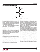
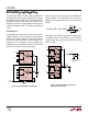
PI FU CTIO S
(GN24 Package)