
Datasheet

LT6555
9
6555f
APPLICATIO S I FOR ATIO
WUUU
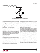
V
REF
voltage to the desired level. The only way to cover the
full common mode voltage range of V
–
+ 1V to V
+
– 1V is
to shift V
REF
up or down. Note that on a single supply, the
unclamped input range limits the output low swing to 2V
(1V multiplied by the internal gain of 2).
The V
REF
pin can also be directly driven with a DC source.
Bypassing the V
REF
pin is not necessary.
The inputs can be driven beyond the point at which the
output clips so long as input currents are limited to less
than ±10mA. Continuing to drive the input beyond the
output limit can result in increased current drive and
slightly increased swing, but will also increase supply
current and may result in delays in transient response at
larger levels of overdrive.
Layout and Grounding
It is imperative that care is taken in PCB layout in order to
benefit from the very high speed and very low crosstalk of
the LT6555. Separate power and ground planes are highly
recommended and trace lengths should be kept as short
as possible. If input or output traces must be run over a
distance of several centimeters, they should use a con-
trolled impedance with matching series and shunt resis-
tances (nominally 75Ω) to maintain signal fidelity.
Series termination resistors should be placed as close to
the output pins as possible to minimize output capaci-
tance. See the Typical Performance Characteristics sec-
tion for a plot of frequency response with various output
capacitors—only 10pF of parasitic output capacitance
before the series termination resistor causes 6dB of
peaking in the frequency response!
Low ESL/ESR bypass capacitors should be placed as
close to the positive and negative supply pins as possible.
One 4700pF ceramic capacitor is recommended for both
V
+
and V
–
supply busses. Additional 470pF ceramic ca-
pacitors with minimal trace length on each supply pin will
further improve AC and transient response as well as
channel isolation. For high current drive and large-signal
transient applications, additional 1µF to 10µF tantalums
should be added on each supply. The smallest value
capacitors should be placed closest to the package.
If the AGND pins are not connected to ground, they must
be carefully bypassed to maintain minimal impedance
over frequency. Although crosstalk will vary depending
upon board layout, a recommended starting point for
bypass capacitors would be 470pF as close as possible to
each AGND pin with a single 4700pF capacitor in parallel.
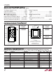
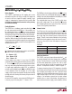
V
REF
40k
40k
6555 F01
V
+
V
–
IN
Figure 1. Simplified Schematic of V
REF
Pin and Input Clamping