
Datasheet

LT6555
10
6555f
To maintain the LT6555’s channel isolation, it is beneficial
to shield parallel input and parallel output traces using a
ground plane or power supply traces. Vias between topside
and backside metal may be required to maintain a low
inductance ground near the part where numerous traces
converge. See Figures 6 and 7 for photos of an optimized
layout.
Input Expansion
In applications with more than two inputs per channel,
multiple LT6555s can be connected by several different
methods. The simplest method is to connect the outputs
after the 75Ω series termination, as shown in Figure 2. The
compromise of this approach is that the internal gain
setting resistors cause a 435Ω shunt across the 75Ω cable
termination, resulting in increased gain error.
APPLICATIO S I FOR ATIO
WUUU
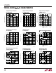
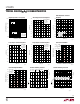
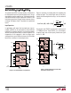
Figure 3. Disabled Amplifiers Load the Cable
Termination with 435Ω Each
Figure 3 illustrates the loading effect of expanding the
number of inputs. The resultant gain error can be calcu-
lated by the following formula using n as the number of
LT6555s:
Gain Error (dB) = 6dB + 20log
435
n–1
Ω
Ω
+
Ω
Ω
⎛
⎝
⎜
⎜
⎜
⎞
⎠
⎟
⎟
⎟
75
75
435
1
75
n
dB
–
For example, two LT6555s would result in a gain error of
–0.74dB per channel. Three LT6555s (i.e., six red inputs,
six green inputs and six blue inputs), would have a gain
error of –1.4dB.
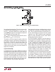
Figure 2. Two LT6555s Build a 4-Input Router
IN1A
IN1B
IN1C
IN1D
CHIP
SELECT
6555 F02
EN
LT6555 #1
75Ω
A
V
= 2
LT6555 #2
74HC04
EN
75Ω
OUT
A
V
= +2
75Ω
CABLE
75Ω
R2
75Ω
6555 F03
360Ω
IN1A
IN1C
IN1B
IN1D
75Ω
1/3 LT6555 #1
1/3 LT6555 #2
360Ω
OFF
360Ω
360Ω
OFF
360Ω
75Ω
75Ω
360Ω
OFF
360Ω
360Ω
ON
⇒
435
n – 1
n = NUMBER OF LT6555s
IN PARALLEL
.
.
.
n