
Datasheet

LT6555
3
6555f
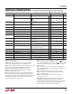
I
S
Supply Current, Per Amplifier R
L
= ∞ 912 mA
● 14 mA
Supply Current, Disabled, Per Amplifier V
EN
= 4V, R
L
= ∞ ● 47 500 µA
V
EN
= Open, R
L
= ∞ ● 42 500 µA
I
EN
Enable Pin Current V
EN
= 0.4V ● –200 –95 µA
V
EN
= 4V ● –75 –21 µA
I
SEL
Select Pin Current V
SEL
= 0.4V ● –50 –5 µA
V
SEL
= 4V ● –50 –1 µA
I
SC
Output Short-Circuit Current R
L
= 0Ω, V
IN
= ±1V ● ±50 ±105 mA
SR Slew Rate ±1V on ±2.5V Output Step (Note 8) 1600 2200 V/µs
–3dB BW Small-Signal –3dB Bandwidth V
OUT
= 200mV
P-P
650 MHz
0.1dB BW Gain Flatness ±0.1dB Bandwidth V
OUT
= 200mV
P-P
120 MHz
FPBW Full Power Bandwidth 2V V
OUT
= 2V
P-P
(Note 9) 250 350 MHz
Full Power Bandwidth 4V V
OUT
= 4V
P-P
(Note 9) 175 MHz
All-Hostile Crosstalk f = 10MHz, V
IN
= 1V
P-P
–72 dB
f = 100MHz, V
IN
= 1V
P-P
–50 dB
Selected Channel to Unselected f = 10MHz, V
IN
= 1V
P-P
–80 dB
Channel Crosstalk f = 100MHz, V
IN
= 1V
P-P
–55 dB
Channel Select Output Transient INA = INB = 0V 200 mV
P-P
Channel-to-Channel Select Time INA = –1V, INB = 1V 8 ns
from 50% SEL to V
OUT
= 0V
t
S
Settling Time 0.1% of V
FINAL
, V
STEP
= 2V 6.5 ns
t
R
,
t
F
Small-Signal Rise and Fall Time 10% to 90%, V
OUT
= 400mV
P-P
520 ps
dG Differential Gain (Note 10) 0.033 %
dP Differential Phase (Note 10) 0.022 Deg
HD2 2nd Harmonic Distortion f = 10MHz, V
OUT
= 2V
P-P
–80 dBc
HD3 3rd Harmonic Distortion f = 10MHz, V
OUT
= 2V
P-P
–70 dBc
ELECTRICAL CHARACTERISTICS
The ● denotes the specifications which apply over the full operating
temperature range, otherwise specifications are at T
A
= 25°C. V
S
= ±5V, R
L
= 150Ω, C
L
= 1.5pF, V
EN
= 0.4V, V
AGND
, V
DGND
, V
VREF
= 0V.
SYMBOL PARAMETER CONDITIONS MIN TYP MAX UNITS
Note 1: Absolute Maximum Ratings are those values beyond which the life
of a device may be impaired.
Note 2: This parameter is guaranteed to meet specified performance
through design and characterization. It is not production tested.
Note 3: As long as output current and junction temperature are kept below
the Absolute Maximum Ratings, no damage to the part will occur.
Depending on the supply voltage, a heat sink may be required.
Note 4: The LT6555C is guaranteed functional over the operating
temperature range of –40°C to 85°C.
Note 5: The LT6555C is guaranteed to meet specified performance from
0°C to 70°C. The LT6555C is designed, characterized and expected to
meet specified performance from –40°C and 85°C but is not tested or QA
sampled at these temperatures. The LT6555I is guaranteed to meet
specified performance from –40°C to 85°C.
Note 6: In order to follow the constraints for 4.5V operation for PSRR
and I
PSRR
testing at ±2.25V, the DGND pin is set to V
–
, the EN pin is set
to V
–
+ 0.4V, and the SEL pin is set to either V
–
+ 0.4V or V
–
+ 4V. At ±6V
and all other cases, DGND is set to ground and the EN and SEL pins are
referenced from it.
Note 7: The V
REF
pin is set to 1V when testing positive swing and –1V
when testing negative swing to ensure that the internal input clamps do
not limit the output swing.
Note 8: Slew rate is 100% production tested using both inputs of
channel 2. Slew rates of channels 1 and 3 are guaranteed through
design and characterization.
Note 9: Full power bandwidth is calculated from the slew rate:
FPBW = SR/(π • V
P-P
)
Note 10: Differential gain and phase are measured using a Tektronix
TSG120YC/NTSC signal generator and a Tektronix 1780R video
measurement set. The resolution of this equipment is better than 0.05%
and 0.05°. Nine identical amplifier stages were cascaded giving an
effective resolution of better than 0.0056% and 0.0056%.