
Datasheet


LT6600-20
8
66002fb
APPLICATIONS INFORMATION
In Figure 3 the LT6600-20 is providing 12dB of gain. The
gain resistor has an optional 62pF in parallel to improve
the passband fl atness near 20MHz. The common mode
output voltage is set to 2V.
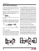
Use Figure 4 to determine the interface between the
LT6600-20 and a current output DAC. The gain, or “trans-
impedance,” is defi ned as A = V
OUT
/I
IN
. To compute the
transimpedance, use the following equation:
A =
402 •R1
R1+ R2
()
Ω
()
By setting R1 + R2 = 402, the gain equation reduces
to A = R1().
The voltage at the pins of the DAC is determined by R1, R2,
the voltage on Pin 7 and the DAC output current. Consider
Figure 4 with R1 = 49.9 and R2 = 348. The voltage at
Pin 7 is 1.65V. The voltage at the DAC pins is given by:
V
DAC
= V
PIN7
•
R1
R1+ R2 + 402
+I
IN
•
R1• R2
R1+ R2
= 26mV + I
IN
• 48.3Ω
I
IN
is I
IN
+
or I
IN
–
. The transimpedance in this example is
50.4.
Evaluating the LT6600-20
The low impedance levels and high frequency operation
ofthe LT6600-20 require some attention to the matching
networks between the LT6600-20 and other devices. The
previous examples assume an ideal (0) source impedance
and a large (1k) load resistance. Among practical ex-
amples where impedance must be considered is the evalu-
ation of the LT6600-20 with a network analyzer. Figure 5
is a laboratory setup that can be used to characterize
the LT6600-20 using single-ended instruments with 50
source impedance and 50 input impedance. For a unity
gain confi guration the LT6600-20 requires a 402 source
resistance yet the network analyzer output is calibrated
for a 50 load resistance. The 1:1 transformer, 53.6
and 388 resistors satisfy the two constraints above.
The transformer converts the single-ended source into a
differential stimulus. Similarly, the output of the LT6600-20
will have lower distortion with larger load resistance yet
the analyzer input is typically 50. The 4:1 turns (16:1
impedance) transformer and the two 402 resistors of
Figure 5, present the output of the LT6600-20 with a 1600
differential load, or the equivalent of 800 to ground at
each output. The impedance seen by the network analyzer
input is still 50, reducing refl ections in the cabling be-
tween the transformer and analyzer input.
Differential and Common Mode Voltage Ranges
The differential amplifi ers inside the LT6600-20 contain
circuitry to limit the maximum peak-to-peak differential
voltage through the fi lter. This limiting function prevents
excessive power dissipation in the internal circuitry and
provides output short-circuit protection. The limiting
function begins to take effect at output signal levels above
2V
P-P
and it becomes noticeable above 3.5V
P-P
. This is
illustrated in Figure 6; the LT6600-20 was confi gured with
unity passband gain and the input of the fi lter was driven
with a 1MHz signal. Because this voltage limiting takes
Figure 4 Figure 5
–
+
0.1µF
3.3V
–
+
LT6600-20
3
4
1
0.01µF
CURRENT
OUTPUT
DAC
7
2
8
5
V
OUT
+
V
OUT
–
66002 F04
6
R2
R1
I
IN
–
I
IN
+
R2
R1
–
+
0.1µF
0.1µF
2.5V
–2.5V
–
+
LT6600-20
3
4
1
7
2
8
5
6
66002 F05
402
402
NETWORK
ANALYZER
INPUT
50
COILCRAFT
TTWB-16A
4:1
NETWORK
ANALYZER
SOURCE
COILCRAFT
TTWB-1010
1:1
50
53.6
388
388