
Datasheet


Table Of Contents
- Features
- Applications
- Description
- Typical Application
- Absolute Maximum Ratings
- Pin Configuration
- Order Information
- Available Options
- Electrical Characteristics
- Typical Performance Characteristics
- Pin Functions
- Block Diagrams
- Applications Information
- Typical Applications
- Package Description
- Revision History
- Typical Application
- Related Parts
LT6654
10
6654fd
For more information www.linear.com/LT6654
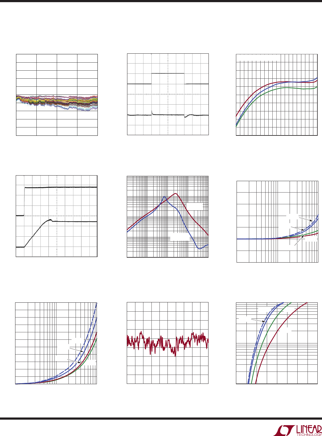
Typical perForMance characTerisTics
5V Load Regulation (Sourcing)
5V Load Regulation (Sinking)
5V Output Noise 0.1Hz to 10Hz
5V Minimum V
IN
to V
OUT
Differential (Sourcing)
5V Output Voltage Temperature
Drift
5V Turn-On Characteristics
5V Output Impedance
vs Frequency
TEMPERATURE (°C)
–60 0 80604020–40 –20 120100
4.993
4.994
4.995
4.996
4.998
4.997
5.002
REFERENCE VOLTAGE (V)
5.003
5.000
4.999
5.001
6654 G28
140
THREE TYPICAL PARTS
50µs/DIV
GND
GND
V
OUT
2V/DIV
V
IN
2V/DIV
6654 G29
C
LOAD
= 1µF
OUTPUT CURRENT (mA)
0.1 1
–20
10
0
OUTPUT VOLTAGE CHANGE (ppm)
50
40
30
20
6654 G31
10
–10
125°C
–40°C
25°C
–55°C
OUTPUT CURRENT (mA)
0.1 1
0
60
40
OUTPUT VOLTAGE CHANGE (ppm)
220
120
100
80
140
200
180
160
6654 G32
10
20
–55°C
25°C
–40°C
125°C
OUTPUT NOISE (4µV/DIV)
TIME (1s/DIV)
6654 G33
109876543210
INPUT-OUTPUT VOLTAGE (mV)
0 50 100 150 200 250 300 350
0.1
OUTPUT CURRENT (mA)
1
10
6654 G34
400
125°C
–40°C
–55°C
25°C
FREQUENCY (kHz)
0.1 1 10 100
0.01
0.1
1
10
OUTPUT IMPEDANCE (Ω)
100
6654 G30
1000
C
L
= 10µF
C
L
= 1µF
The characteristic curves are similar across the
LT6654 family. Curves from the LT6654-1.25, LT6654-2.5 and the LT6654-5 represent the full range of typical performance of all
voltage options. Characteristic curves for other output voltages fall between these curves and can be estimated based on their output.
2.5V Load Transient Response
(Sinking)
50µs/DIV
0mA
V
OUT
20mV/DIV/AC
2.5V/DC
6654 G27
C
LOAD
= 1µF
I
OUT
5mA
2.5V Long Term Drift (LS8)
TIME (HOURS)
0
PPM
150
–90
–60
–30
30
60
90
120
0
–150
–120
1000500
6654 G38
20001500