
Datasheet


LT6656
13
6656fc
For more information www.linear.com/LT6656
I
L
= 0
V
OUT
10mV/DIV
I
L
= 5µA
3.25V
V
IN
2.75V
5ms/DIV
6656 F07
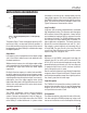
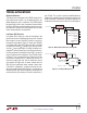
Figure 7. Detailed Output Response to a 0.5V Input Step,
C
IN
= C
L
= 1µF
APPLICATIONS INFORMATION
The photo in Figure 7 shows the output response to a 0.5V
input step in both a no-load and 5µA load condition. In
the no-load condition only the bias current of the internal
bandgap reference (about 400nA) is available to discharge
the output capacitor.
Output Noise
Low frequency noise is proportional to the output voltage
and is insensitive to output current and moderate levels
of output capacitance.
Wideband noise increases less with higher output voltage
and is proportional to the bandwidth of the output stage,
increasing with higher load current and lower output
capacitance.
Peaking in the noise response is another factor contribut
-
ing to the output noise level for a given frequency range.
Noise peaking
can be reduced by increasing
the size of the
output capacitor when driving heavier loads, or conversely,
reducing the size of the output capacitor when driving
lighter loads. Noise plots in the Typical Performance Curves
section show noise spectrum with various load currents
and output capacitances.
Internal Protection
The LT6656 incorporates several internal protection
features that make it ideal for use in battery powered
systems. Reverse input protection limits the input cur
-
rent to typically less than 40µA when either the LT6656
or the batter
y is installed backwards. In systems where
the
output can be held up by a backup battery with the
input pulled to ground, the reverse output protection of
the LT6656 limits the output current to typically less than
30µA. The current versus reverse voltage is shown in the
Typical Performance Characteristics section.
Long-Term Drift
Long-term drift cannot be extrapolated from accelerated
high temperature testing. This erroneous technique gives
drift numbers that are wildly optimistic. A more realistic
way to determine long-term drift is to measure it over the
time interval of interest. The LT6656 drift data was taken
over 100 parts that were soldered onto PC boards in a
typical application configuration. The boards were then
placed into a constant temperature oven with T
A
= 30°C,
their outputs scanned regularly and measured with an
8.5 digit DVM. The parts chosen in the Long Term Drift
curves in the Typical Performance Characteristics section
represent high, low and typical units.
Hysteresis
Hysteresis on the LT6656 is measured in two steps, for
example, from 25°C to –40°C to 25°C, then from 25°C to
85°C to 25°C, for the industrial temperature range. After
preconditioning by one thermal cycle, this two-step cycle
is repeated several times and the maximum hysteresis
from all the partial cycles is noted.
Results over both commercial and industrial temperature
ranges are shown in Figure 8 and Figure 9. The parts cycled
over the higher temperature range have a higher hysteresis
than those cycled over the lower range.
Power Dissipation
The LT6656 will not exceed the maximum junction tem
-
perature when operating within its specified temperature
range of –40°C to 85°C, maximum input voltage of 18V
and specified load current of 5mA.
IR Reflow Shift
The different expansion and contraction rates of the mate
-
rials that make up the LT6656 package may induce small
stresses on the die that can cause the output to shift during