
Datasheet

LT8302
11
Rev E
For more information www.analog.com
APPLICATIONS INFORMATION
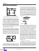
Output Voltage
The R
FB
and R
REF
resistors as depicted in the Block
Diagram are external resistors used to program the out-
put voltage. The LT8302 operates similar to traditional
current mode switchers, except in the use of a unique
flyback pulse sense circuit and a sample-and-hold error
amplifier, which sample and therefore regulate the isolated
output voltage from the flyback pulse.
Operation is as follows: when the power switch M1 turns
off, the SW pin voltage rises above the V
IN
supply. The
amplitude of the flyback pulse, i.e., the difference between
the SW pin voltage and V
IN
supply, is given as:
V
FLBK
= (V
OUT
+ V
F
+ I
SEC
• ESR) • N
PS
V
F
= Output diode forward voltage
I
SEC
= Transformer secondary current
ESR = Total impedance of secondary circuit
N
PS
= Transformer effective primary-to-secondary
turns ratio
The flyback voltage is then converted to a current, I
RFB
,
by the R
FB
resistor and the flyback pulse sense circuit
(M2 and M3). This current, I
RFB
, also flows through the
R
REF
resistor to generate a ground-referred voltage. The
resulting voltage feeds to the inverting input of the sam
-
ple-and-hold error amplifier. Since the sample-and-hold
error amplifier samples the voltage when the secondary
current is zero, the (I
SEC
• ESR) term in the V
FLBK
equation
can be assumed to be zero.
The internal reference voltage, V
REF
, 1.00V, feeds to the
noninverting input of the sample-and-hold error ampli-
fier. The relatively high gain in the overall loop causes the
voltage at the R
REF
pin to be nearly equal to the internal
reference voltage V
REF
. The resulting relationship between
V
FLBK
and V
REF
can be expressed as:
V
FLBK
R
FB
⎛
⎝
⎜
⎞
⎠
⎟
•R
REF
= V
REF
or
V
FLBK
= V
REF
•
R
FB
R
REF
⎛
⎝
⎜
⎞
⎠
⎟
V
REF
= Internal reference voltage 1.00V
Combination with the previous V
FLBK
equation yields an
equation for V
OUT
, in terms of the R
FB
and R
REF
resistors,
transformer turns ratio, and diode forward voltage:
V
OUT
= V
REF
•
R
FB
R
REF
⎛
⎝
⎜
⎞
⎠
⎟
•
1
N
PS
⎛
⎝
⎜
⎞
⎠
⎟
– V
F
Output Temperature Compensation
The first term in the V
OUT
equation does not have tem-
perature dependence, but the output diode forward volt-
age, V
F
, has a significant negative temperature coefficient
(–1mV/°C to –2mV/°C). Such a negative temperature coef-
ficient produces approximately 200mV to 300mV voltage
variation on the output voltage across temperature.
For higher voltage outputs, such as 12V and 24V, the
output diode temperature coefficient has a negligible
effect on the output voltage regulation. For lower voltage
outputs, such as 3.3V and 5V, however, the output diode
temperature coefficient does count for an extra 2% to 5%
output voltage regulation.
The LT8302 junction temperature usually tracks the out
-
put diode junction temperature to the first order. To com-
pensate the negative temperature coefficient of the output
diode, a resistor, R
TC
, connected between the TC and R
REF
pins generates a proportional-to-absolute-temperature
(PTAT) current. The PTAT current is zero at 25°C, flows
into the R
REF
pin at hot temperature, and flows out of the
R
REF
pin at cold temperature. With the R
TC
resistor in
place, the output voltage equation is revised as follows:
V
OUT
= V
REF
•
R
FB
R
REF
•
1
N
PS
– V
F
TO
( )
– V
TC
/ T
( )
•
T –TO
( )
•
R
FB
R
TC
•
1
N
PS
– V
F
/ T
( )
• T–TO
( )
TO=Room temperature 25°
°
C
V
F
/ T
( )
= Output diode forward voltage
temperature coefficient
V
TC
/ T
( )
= 3.35mV/ C
Downloaded from Arrow.com.Downloaded from Arrow.com.Downloaded from Arrow.com.Downloaded from Arrow.com.Downloaded from Arrow.com.Downloaded from Arrow.com.Downloaded from Arrow.com.Downloaded from Arrow.com.Downloaded from Arrow.com.Downloaded from Arrow.com.Downloaded from Arrow.com.