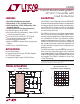
LT8582 Dual 3A Boost/Inverting/SEPIC DC/DC Converter with Fault Protection DESCRIPTION FEATURES n n n n n n n n n n n Dual 42V, 3A Combined Power Switch Master/Slave (1.7A/1.3A) Switch Design Wide Input Range: 2.5V to 22V Operating, 40V Maximum Transient Power Good Pin for Event Based Sequencing Switching Frequency Up to 2.5MHz Each Channel Easily Configurable as a Boost, SEPIC, Inverting or Flyback Converter Low VCESAT Switch: 270mV at 2.
LT8582 ABSOLUTE MAXIMUM RATINGS PIN CONFIGURATION (Note 1) VIN1 Voltage ............................................... –0.3V to 40V SWA1/SWB1 Voltage.................................. –0.4V to 42V RT1 Voltage ................................................. –0.3V to 5V SS1 Voltage .............................................. –0.3V to 2.5V FBX1 Voltage................................................ –0.3V to 5V VC1 Voltage .................................................. –0.3V to 2V SHDN1 Voltage ..
LT8582 ELECTRICAL CHARACTERISTICS The l denotes the specifications which apply over the full operating temperature range, otherwise specifications are at TA = 25°C. VIN = 5V, VSHDN = VIN, unless otherwise noted (Note 2). Specifications are identical for both channels unless noted otherwise. PARAMETER CONDITIONS MIN l Minimum Input Voltage VIN VIN Overvoltage Lockout TYP MAX UNITS 2.3 2.5 V 22.2 24.5 27 V Positive Feedback Voltage l 1.185 1.204 1.
LT8582 ELECTRICAL CHARACTERISTICS The l denotes the specifications which apply over the full operating temperature range, otherwise specifications are at TA = 25°C. VIN = 5V, VSHDN = VIN, unless otherwise noted (Note 2). Specifications are identical for both channels unless noted otherwise. PARAMETER CONDITIONS MIN TYP MAX UNITS SHDN Pin Bias Current VSHDN = 3V VSHDN = 1.3V VSHDN = 0V 10.1 45 12.1 0 65 14.1 0.1 μA μA μA CLKOUT Output Voltage High 1mA out of CLKOUT Pin 1.9 2.1 2.
LT8582 TYPICAL PERFORMANCE CHARACTERISTICS Switch Current Limit vs Duty Cycle TA = 25°C, unless otherwise noted. Switch Current Sharing Switch Saturation Voltage 350 5 1.0 VSW1 = VSW2 0.9 3 2 1 0.8 250 0.7 ISWB/ISWA (A/A) 4 SATURATION VOLTAGE (mV) SWA + SWB CURRENT (A) 300 200 150 20 30 40 50 60 70 DUTY CYCLE (%) 80 0.1 0 90 0.5 0 2.5 1.
LT8582 TYPICAL PERFORMANCE CHARACTERISTICS TA = 25°C, unless otherwise noted. Positive Feedback Voltage Gate Pin Current (VGATE = 5V) 1000 Active/Lockout Threshold 1.220 1.40 1.38 900 1.215 600 500 400 300 200 1.36 SHDN VOLTAGE (V) 700 FBX VOLTAGE (V) GATE PIN CURRENT (μA) 800 1.210 1.205 1.200 1.30 1.28 SHDN FALLING 1.26 1.22 0 0 0.25 0.75 1 0.5 SS VOLTAGE (V) 1.25 1.5 1.190 –50 –25 0 1.
LT8582 PIN FUNCTIONS (CH1/CH2) FBX1, FBX2 (Pin 6/Pin 7): Positive and Negative Feedback Pins. For an inverting or noninverting output converter, tie a resistor from the FBX pin to VOUT according to the following equations: ⎛V – 1.204V ⎞ R FBX = ⎜ OUT ⎟⎠ ; Noninverting ⎝ 83.3μA Converter || +7mV ⎞ ⎛|| V R FBX = ⎜ OUT ; Inverting Converter ⎝ 83.3μA ⎟⎠ VC1, VC2 (Pin 5/Pin 8): Error Amplifier Output Pins. Tie external compensation network to these pins. GATE1, GATE2 (Pin 4/Pin 9): PMOS Gate Drive Pins.
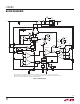
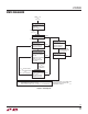
LT8582 BLOCK DIAGRAM RFBX FBX1 OPTIONAL D1 L1 M1 VIN CIN COUT1 RPG GATE1 VOUT COUT2 RGATE PG1 1mA SOFT-START VC1 2.1V + START-UP AND FAULT LOGIC – + 1.84V 250k – CSS VIN1 + – 22.2V (MIN) – + – – UVLO + + DRIVER SR1 R A3 S Q2 SWA1 28mΩ Q1 Q + A1 14.5k RS 22mΩ A4 – FBX1 SWB1 7#& t + COMPARATOR 1.204V REFERENCE 65mV TD ~ 30ns – – 1.31V 1.
LT8582 STATE DIAGRAM SHDN1 7 03 7*/ 7 CHIP OFF t "-- 48*5$)&4 %*4"#-&% t *("5& 0'' t '"6-5T $-&"3&% SHDN1 7 "/% 7*/ 7 INITIALIZE t 44 1*/ 16--&% -08 '"6-5 44 1*/ N7 FAULT DETECTED SOFT-START t *("5& &/"#-&% t 44 1*/ $)"3(&4 61 t 48*5$)&3 &/"#-&% '"6-5 44 1*/ 7 "/% /0 '"6-5 $0/%*5*0/4 45*-- %&5&$5&% SAMPLE MODE t 2 "/% 2 48*5$)&4 '03$&% 0/ &7&3: $:$-& '03 "5 -&"45 .*/*.6. 0/ 5*.
LT8582 OPERATION OPERATION – OVERVIEW The LT8582 uses a constant frequency, current mode control scheme to provide excellent line and load regulation. Each channel’s undervoltage lockout (UVLO) function, together with soft-start and frequency foldback, offer a controlled means of starting up. Fault features are incorporated into each channel of the LT8582 to facilitate the detection of output shorts, overvoltage and overtemperature conditions.
LT8582 OPERATION Sample Mode Sample mode is the mechanism used by the LT8582 to aid in the detection of output shorts. It refers to a state of the LT8582 where the master and slave power switches (Q1 and Q2) are turned on for a minimum period of time every clock cycle (or every few clock cycles in frequency foldback) in order to sample the inductor current.
LT8582 OPERATION Refer to the State Diagram (Figure 2) for the following description of the LT8582’s operation during a fault event. When a fault is detected on a channel, the LT8582 disables the CLKOUT pin for that channel, turns off the power switches for that channel and the GATE pin for that channel becomes high impedance. The external PMOS, M1, is turned off by the external RGATE resistor (see Block Diagram).
LT8582 APPLICATIONS INFORMATION Boost Converter Component Selection D1 30V, 2A L1 4.7μH VIN 5V PARAMETERS/EQUATIONS OPTIONAL VOUT 12V 0.8A M1 COUT1 10μF SWA Table 1. Boost Converter Design Equations 6.04k 100k CIN 4.7μF RT 53.6k SWB Step 2: DC DC ≅ Step 3: L1 FBX LT8582 GATE SHDN CHx PG CLKOUT RT VC SYNC GND Choose VIN, VOUT and fOSC to calculate equations below. RFBX 130k VIN 215k Step 1: Inputs SS COUT2 10μF 47pF 0.1μF VOUT – VIN + 0.5V VOUT + 0.5V – 0.3V L TYP = (VIN – 0.
LT8582 APPLICATIONS INFORMATION SEPIC Converter Component Selection – Coupled or Uncoupled Inductors VOUT 5V 1A(VIN >12V) s SWA SWB LT8582 FBX CHx SHDN GATE CIN 10μF RT 107K PG CLKOUT RT VC Step 2: DC Choose VIN, VOUT and fOSC to calculate equations below. DC ≅ L2 6.8μH Step 3: L RFBX 45.3k VIN 100k PARAMETERS/EQUATIONS Step 1: Inputs D1 40V, 2A s VIN 3V TO 19V C1 2.2μF L1 6.8μH Table 2. SEPIC Design Equations COUT 22μF ×2 SYNC GND SS 47pF 0.1μF VOUT + 0.5V VIN + VOUT + 0.5V – 0.
LT8582 APPLICATIONS INFORMATION Dual Inductor Inverting Converter Component Selection – Coupled or Uncoupled Inductors s PARAMETERS/EQUATIONS Step 1: Inputs L2 4.7μH VOUT –12V 550mA s VIN 5V C1 2.2μF L1 4.7μH Table 3. Dual Inductor Inverting Design Equations Step 2: DC D1 30V, 2A SWA SWB VIN LT8582 FBX CHx GATE SHDN 100k CIN 4.7μF RT 53.6K PG CLKOUT RT VC SYNC GND SS | VOUT | + 0.5V VIN + | VOUT | +0.5V – 0.3V L TYP = (VIN – 0.3V) • DC fOSC • 1A (1) L MIN = (VIN – 0.
LT8582 APPLICATIONS INFORMATION LAYOUT GUIDELINES FOR LT8582 Boost Topology Specific Layout Guidelines General Layout Guidelines • Keep length of loop (high speed switching path) governing switch, diode D1, output capacitor COUT1 and ground return as short as possible to minimize parasitic inductive spikes during switching. • To improve thermal performance, solder the exposed ground pad of the LT8582 to the ground plane, with multiple vias in and around the pad connecting to additional ground planes.
LT8582 APPLICATIONS INFORMATION Power and Thermal Calculations THERMAL CONSIDERATIONS For the LT8582 to deliver its full output power, it is imperative that a good thermal path be provided to dissipate the heat generated within the package. This can be accomplished by taking advantage of the thermal pad on the underside of the chip. It is recommended that multiple vias in the printed circuit board be used to conduct heat away from the chip and into copper planes with as much area as possible.
LT8582 s L3 s APPLICATIONS INFORMATION L4 D2 C2 COUT2 CPWR2 VOUT2 + VIN – CLKOUT2 SYNC1 13 12 14 11 15 10 16 9 17 8 18 7 19 6 20 5 21 4 22 3 23 2 24 1 CVIN2 GND CVIN1 25 VOUT1 CPWR1 COUT1 s D1 s C1 L1 L2 8582 F09 Figure 9. Suggested Component Placement for SEPIC and Dual Inductor Inverting Topologies.
LT8582 APPLICATIONS INFORMATION Table 4 calculates the power dissipation of one channel of the LT8582 for a particular boost application (VIN = 5V, VOUT = 12V, IOUT = 0.8A, fOSC = 1.5MHz, VD = 0.5V, VCESAT = 0.270V).
LT8582 APPLICATIONS INFORMATION SWITCHING FREQUENCY There are several considerations in selecting the operating frequency of the converter. The first is staying clear of sensitive frequency bands, which cannot tolerate any spectral noise. For example, in RF communication products with a 455kHz IF, switching above 600kHz is desired. Communication products with sensitivity to 1.1MHz would require to set the switching frequency to 1.5MHz or higher.
LT8582 APPLICATIONS INFORMATION is close to its regulation voltage. This method allows the PG pin to disable multiple ICs. Refer to Figure 10 for the necessary connections. Alternatively, the PG pin may be used to pull the SS pin of another switching regulator low, preventing the other regulator from switching.
LT8582 APPLICATIONS INFORMATION Single Inductor Inverting Topology HOT-PLUG If there is a need to use just one inductor to generate a negative output voltage whose magnitude is greater than VIN, the single inductor inverting topology (shown in Figure 12) can be used. Since the master and slave switches are isolated by a Schottky diode, the current spike through C1 will flow only through the slave switch, preventing the current comparator, (A4 in the Block Diagram) from false tripping.
LT8582 APPENDIX INDEPENDENT CHANNELS Either channel may be used independently of the other channel. To disable one channel, drive SHDN of that channel low. Activating or deactivating one channel will not alter the functionality of the other channel. Duty cycle equations for several common topologies are given below where VD is the diode forward voltage drop and VCESAT is the collector to emitter saturation voltage of the switch.
LT8582 APPENDIX use a toroidal or shielded inductor. See Table 5 for a list of inductor manufacturers. Table 5. Inductor Manufacturers where LBOOST = L1 for boost topologies (see Figure 5) LDUAL = L1 = L2 for coupled dual inductor topologies (see Figures 6 and 7) Coilcraft MSD7342 XAL6060 Series www.coilcraft.com Vishay IHLP-2020BZ-01 IHLP-2525CZ-01 Series www.vishay.com LDUAL = L1 || L2 for uncoupled dual inductor topologies (see Figures 6 and 7) WÜRTH WE-PD WE-DD WE-TDC Series www.we-online.
LT8582 APPENDIX Maximum Inductance Excessive inductance can reduce current ripple to levels that are difficult for the current comparator (A4 in the Block Diagram) to easily distinguish the peak current. This causes duty cycle jitter and/or poor regulation. The maximum inductance can be calculated by: Note that these equations offer conservative results for the required inductor current ratings.
LT8582 APPENDIX and one at the input to the power path (see the equation for CPWR in Table 1, Table 2 and Table 3). A 4.7μF to 20μF input capacitor is sufficient for most applications. Table 6 shows a list of several ceramic capacitor manufacturers. Consult the manufacturers for detailed information on their entire selection of ceramic parts. Table 6. Ceramic Capacitor Manufacturers TDK www.tdk.com Murata www.murata.com Taiyo Yuden www.t-yuden.com Kemet www.kemet.
LT8582 APPENDIX Table 7 shows a list of several discrete PMOS manufacturers. Consult the manufacturers for detailed information on their entire selection of PMOSs. Table 7. Discrete PMOS Manufacturers Vishay www.vishay.com ON Semiconductor www.onsemi.com Fairchild Semiconductor www.fairchildsemi.com Diodes Incorporated www.diodes.com VOUT AC-COUPLED 500mV/DIV IL 1A/DIV ILOAD 400mA/DIV 100μs/DIV 8582 F14b Figure 14b.
LT8582 APPENDIX Error Amp Pole: – + VOUT gmp IVIN M t 7IN VOUT RESR t *VIN CPL + CF RC RO R1 R2 FBX – 8582 F15 Error Amp Zero: 1 Z1= 2 • π • R C • CC ESR Zero: R2 CC Z2 = CC: COMPENSATION CAPACITOR COUT: OUTPUT CAPACITOR CPL: PHASE LEAD CAPACITOR CF: HIGH FREQUENCY FILTER CAPACITOR gma: TRANSCONDUCTOR ERROR AMPLIFIER INSIDE THE CHIP gmp: POWER STAGE TRANSCONDUCTANCE AMPLIFIER RC: COMPENSATION RESISTOR RL: OUTPUT RESISTANCE DEFINED AS VOUT/ILOADMAX RO: OUTPUT RESISTANCE OF gma R1, R2: OUTPUT
LT8582 APPENDIX The current mode zero (Z3) is a right half plane zero which can be an issue in feedback control design, but is manageable with proper external component selection. 0 140 120 GAIN (dB) 100 –90 80 –135 –180 60 50° AT 5kHz 40 GAIN 20 Table 8.
LT8582 TYPICAL APPLICATIONS 1.5MHz, 5V to ±12V Boost and Inverting Converter Can Survive Output Shorts L1 4.7μH D1 M1 CIN1 4.7μF COUT1 10μF SWA1 SWB1 100k SHDN1 PG1 130k GATE1 LT8582 COUT2 10μF VC1 SS1 CLKOUT1 RT1 6.49k 47pF 0.1μF 53.6k 4.7nF 53.6k 2.2nF GND SYNC2 215k PG2 RT2 SHDN2 SS2 VIN2 VC2 0.1μF 47pF 14.7k 100 3.2 90 2.8 80 2.4 70 2.0 60 1.6 50 1.2 40 0.8 30 0.4 20 0 COUT3 10μF GATE2 143k 0.1 0.4 0.3 0.2 LOAD CURRENT (A) L2 4.7μH 0 0.
LT8582 TYPICAL APPLICATIONS VFD (Vacuum Fluorescent Display) and Filament Power Supply Switches at 1MHz D6 VOUT1 100V C6 80mA* 2.2μF D5 C4 2.2μF D4 VOUT2 66V C5 120mA* 2.2μF D3 C3 2.2μF L1 22μH VIN 9V TO 16V D2 CIN1 4.7μF D1 CIN1, CIN2: 4.7μF, 25V, X7R, 1206 C1 TO C6: 2.2μF, 50V, X7R, 1206 C7: 2.
LT8582 TYPICAL APPLICATIONS Tracking ±15V Supplies from a 2.7V to 5.5V Input L1 10μH VIN 2.7V TO 5.5V D1 CIN1 10μF 49.9k SWA1 SWB1 6.04k FBX1 VIN1 SHDN1 100k VOUT1 15V 0.3A(VIN = 2.7V) 0.42A(VIN = 3.6V) 0.56A(VIN = 4.5V) 0.69A(VIN = 5.5V) PG1 FBX2 GATE1 LT8582 COUT1 10μF ×2 VC1 SYNC1 SS1 CLKOUT1 RT1 6.65k 0.1μF 107k CLKOUT2 CIN1, CIN2: 10μF, 16V, X7R, 1206 COUT1, COUT2: 10μF, 25V, X7R, 1210 C1: 4.7μF, 50V, X7R, 1206 D1, D2: DIODES INC.
LT8582 TYPICAL APPLICATIONS SuperCap Backup Power VOUT VIN (VIN > 11.4V) 11V (VIN < 11.4V) M1 C1 2.2μF L1 5μH 6.04k D1 VOUT1 10V s VIN 12V ±5% CIN1 4.7μF L2 5μH s SWA1 100k 73.2k SWB1 VIN1 FBX1 PG1 GATE1 SHDN1 COUT1 4.7μF 130k COUT2 10μF VC1 LT8582 11k SS1 SYNC1 15.4k 80.6k CLKOUT1 100pF 0.47μF RT1 1.2k 1/4W CS1 60F 1.2k 1/4W CS2 60F 1.2k 1/4W CS3 60F 1.2k 1/4W CS4 60F 1nF GND CLKOUT2 80.6k SYNC2 VOUT1 100k 3.3nF RT2 PG2 SS2 SHDN2 VC2 VIN2 0.47μF 100pF 12.
LT8582 TYPICAL APPLICATIONS 12V and 5V Sequenced Outputs from a 3V to 19V Input* C1 2.2μF L1 8.2μH D1 CIN1 10μF SWA1 SWB1 s L2 8.2μH VIN1 SHDNSYS 130k *FOR SYSTEM LEVEL DIAGRAM, SEE FIGURE 10 FBX1 10k 10k SHDN1 M1 VOUT1 12V 0.3A (VIN = 3V) 0.5A (VIN = 5V) 1A (VIN = 12V) s VIN 3V to 19V 115k PG1 M2 GATE1 LT8582 COUT1 10μF ×2 VC1 SYNC1 SS1 CLKOUT1 RT1 CLKOUT2 47pF 20k 0.1μF 107k 1.5nF 107k 1.5nF GND SYNC2 100k PG2 RT2 SHDN2 VIN2 47pF 0.1μF 14.
LT8582 PACKAGE DESCRIPTION Please refer to http://www.linear.com/designtools/packaging/ for the most recent package drawings. DKD Package 24-Lead Plastic DFN (7mm × 4mm) (Reference LTC DWG # 05-08-1864 Rev Ø) 0.70 p 0.05 4.50 p 0.05 6.43 p0.05 2.64 p0.05 3.10 p 0.05 PACKAGE OUTLINE 0.50 BSC 0.25 p 0.05 5.50 REF RECOMMENDED SOLDER PAD LAYOUT APPLY SOLDER MASK TO AREAS THAT ARE NOT SOLDERED 7.00 p0.10 13 R = 0.115 TYP 24 R = 0.05 TYP 0.40 p 0.10 6.43 p0.10 4.00 p0.10 2.64 p0.
LT8582 TYPICAL APPLICATION 700kHz SEPIC and Inverting Converter Generates ±5V Outputs from a 3V to 19V Input C1 2.2μF L1 4.7μH VOUT1 5V 0.7A (VIN = 3V) 1.4A (VIN = 9V) 1.5A (VIN = 16V) D1 s VIN 3V to 19V CIN1 22μF SWA1 SWB1 s L2 4.7μH SHDN1 100k PG1 EFFICIENCY (%) FBX1 LT8582 GATE1 COUT1 22μF ×2 VC1 SYNC1 SS1 CLKOUT1 RT1 11.8k 47pF 0.1μF 115k CLKOUT2 VIN2 115k 2.2nF RT2 0.1μF 3.5 60 3.0 50 2.5 40 2.0 30 1.5 20 1.0 10 0.5 0.2 0.4 0.6 0.8 1 1.