
Datasheet

LT8582
3
8582f
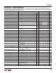
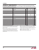
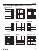
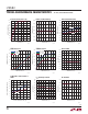
ELECTRICAL CHARACTERISTICS
PARAMETER CONDITIONS MIN TYP MAX UNITS
Minimum Input Voltage V
IN
l
2.3 2.5 V
V
IN
Overvoltage Lockout 22.2 24.5 27 V
Positive Feedback Voltage
l
1.185 1.204 1.220 V
Negative Feedback Voltage
l
2 7 16 mV
Positive FBX Pin Bias Current V
FBX
= Positive Feedback Voltage, Current into Pin
l
81 83.3 85 µA
Negative FBX Pin Bias Current V
FBX
= Negative Feedback Voltage, Current out of Pin
l
81 83.3 85.5 µA
Error Amp Transconductance ∆I = 10A 280 µmhos
Error Amp Voltage Gain 80 V/V
Quiescent Current V
SHDN
= 2.5V, Not Switching 2.1 2.5 mA
Quiescent Current in Shutdown V
SHDN
= 0 0 1 µA
Reference Line Regulation 2.5V ≤ V
IN
≤ 20V 0.01 0.05 %/V
Switching Frequency, f
OSC
R
T
= 31.6k
R
T
= 407k
l
l
2.125
170
2.5
200
2.875
230
MHz
kHz
Switching Frequency in Foldback Compared to Normal f
OSC
1/6 ratio
Switching Frequency Range Free-Running or Synchronizing
l
200 2500 kHz
SYNC High Level for Sync
l
1.3 V
SYNC Low Level for Sync
l
0.4 V
SYNC Clock Pulse Duty Cycle V
SYNC
= 0V to 2V 20 80 %
Recommended Min SYNC Ratio f
SYNC
/f
OSC
3/4 ratio
Minimum Off-Time 45 ns
Minimum On-Time 55 ns
SWA Current Limit Minimum Duty Cycle
Maximum Duty Cycle
l
l
1.8
1.3
2.4
1.8
3
2.5
A
A
SWA FAULT Current Limit Minimum Duty Cycle
Maximum Duty Cycle
l
l
2.2
1.6
2.8
2.3
3.5
3.0
A
A
SW Current Sharing, I
SWB
/I
SWA
SWA and SWB Tied Together 0.79 A/A
SWA + SWB Current Limit Minimum Duty Cycle, I
SWB
/I
SWA
= 0.79
Maximum Duty Cycle, I
SWB
/I
SWA
= 0.79
l
l
3.3
2.3
4.3
4.1
5.4
4.5
A
A
SWA + SWB FAULT Current Limit Minimum Duty Cycle, I
SWB
/I
SWA
= 0.79
Maximum Duty Cycle, I
SWB
/I
SWA
= 0.79
l
l
4
2.8
5
4
6.3
5.4
A
A
Switch V
CESAT
I
SWA
+ I
SWB
= 2.75A 270 mV
SWA Leakage Current V
SWA
= 5V, V
SHDN
= 0 0.01 1 µA
SWB Leakage Current V
SWB
= 5V, V
SHDN
= 0 0.01 1 µA
SS Charge Current V
SS
= 30mV, Current Flows out of SS Pin
l
5.7 8.8 11.7 µA
SS Discharge Current Part in FAULT, V
SS
= 2.1V, Current Flows into SS Pin
l
5.7 8.8 11.7 µA
SS High Detection Voltage Part in FAULT
l
1.65 1.84 2 V
SS Low Detection Voltage Part Exiting FAULT
l
15 55 100 mV
SHDN Minimum Input Voltage High Active Mode, SHDN Rising
Active Mode, SHDN Falling
l
l
1.26
1.21
1.31
1.27
1.4
1.35
V
V
SHDN Input Voltage Low Shutdown Mode
l
0.3 V
The l denotes the specifications which apply over the full operating
temperature range, otherwise specifications are at T
A
= 25°C. V
IN
= 5V, V
SHDN
= V
IN
, unless otherwise noted (Note 2). Specifications
are identical for both channels unless noted otherwise.