
Datasheet

LT8582
7
8582f
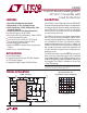
PIN FUNCTIONS
FBX1, FBX2 (Pin 6/Pin 7): Positive and Negative Feedback
Pins. For an inverting or noninverting output converter,
tie a resistor from the FBX pin to V
OUT
according to the
following equations:
R ; Noninverting
Converter
FBX
=
V
OUT
– 1.204V
83.3µA
⎛
⎝
⎜
⎞
⎠
⎟
R
FBX
=
|
|
V
OUT
|
|
+7mV
83.3µA
; Inverting Converter
⎛
⎝
⎜
⎞
⎠
⎟
VC1, VC2 (Pin 5/Pin 8): Error Amplifier Output Pins. Tie
external compensation network to these pins.
GATE1, GATE2 (Pin 4/Pin 9): PMOS Gate Drive Pins. The
GATE pin is a pull-down current source and can be used
to drive the gate of an external PMOS transistor for output
short-circuit protection or output disconnect. The GATE
pin current increases linearly with the SS pin voltage,
with a maximum pull-down current of 1mA at SS voltages
exceeding 550mV. Note that if the SS voltage is greater
than 550mV and the GATE pin voltage is less than 2V, the
GATE pin looks like a 2k impedance to ground. See the
Appendix for more information.
PG1, PG2 (Pin 3/Pin 10): Power Good Indication Pins.
This active high pin indicates that the FBX pin voltage for
the corresponding channel is within 4% of its regulation
voltage (V
FBX
> 1.15V for noninverting outputs or V
FBX
<
65mV for inverting outputs). For most applications, a 4%
change in V
FBX
corresponds to an 8% change in V
OUT
. This
open drain output requires a pull-up resistor to indicate
power good. Also, the status is valid only when SHDN >
1.31V and V
IN
> 2.3V.
VIN1, VIN2 (Pin 2/Pin 11): Input Supply Pins. Must be
locally bypassed.
SWA1, SWA2 (Pin 1/Pin 12): Master Switch Pins. This is
the collector of the internal master NPN power switch for
each channel. SWA is designed to handle a peak collector
current of 1.7A (minimum). Minimize the metal trace area
connected to this pin to minimize EMI.
SWB1, SWB2 (Pin 24/Pin 13): Slave Switch Pins. This is
the collector of the internal slave NPN power switch for
each channel. SWB is designed to handle a peak collector
current of 1.3A (minimum). Minimize the metal trace area
connected to this pin to minimize EMI.
CLKOUT1, CLKOUT2 (Pin 23/Pin 14): Clock Output Pins.
Use these pins to synchronize one or more other ICs to
either channel of the LT8582. Can also be used to syn-
chronize channel 1 or channel 2 of the LT8582 with the
other channel of the LT8582. This pin oscillates at the same
frequency as the internal oscillator of the part or, if active,
the SYNC pin. The CLKOUT pin signal on CH1 is 180° out
of phase with the internal oscillator or SYNC pin and the
duty cycle is fixed at ~50%. The CLKOUT pin signal on
CH2 is in phase with the internal oscillator or SYNC pin
and the duty cycle varies linearly with the part’s junction
temperature. Note that CLKOUT of either channel is only
meant to drive capacitive loads up to 120pF.
SHDN1, SHDN2 (Pin 22/Pin 15): Shutdown Pins. In
conjunction with the UVLO (undervoltage lockout) circuit,
these pins are used to enable/disable the channel and
restart the soft-start sequence. Drive below 0.3V to dis-
able the channel with very low quiescent current. Drive
above 1.31V (typical) to activate the channel and restart
the soft-start sequence. Do not float these pins.
RT1, RT2 (Pin 21/Pin 16): Timing Resistor Pins. Adjusts the
switching frequency of the corresponding channel. Place
a resistor from these pins to ground to set the frequency
to a fixed free running level. Do not float these pins.
SS1, SS2 (Pin 20/Pin 17): Soft-Start Pins. Place a soft-
start capacitor here. Upon start-up, the SS pins will be
charged by a (nominally) 250k resistor to ~2.1V. During
a fault, the SS pin for the corresponding channel will be
slowly charged up and discharged as part of a timeout
sequence (see the State Diagram for more information).
SYNC1, SYNC2 (Pin 19/Pin 18): Use to synchronize the
switching frequency of a channel to an outside clock. The
high voltage level of the clock must exceed 1.3V and the
low level must be less than 0.4V. Drive these pins to less
than 0.4V to revert to the internal free running clock for the
corresponding channel. See the Applications Information
section for more information.
GND (Exposed Pad Pin 25): Ground. Exposed pad must
be soldered directly to local ground plane.
(CH1/CH2)