
Datasheet


LT8608/LT8608B
16
Rev. D
For more information www.analog.com
APPLICATIONS INFORMATION
For some applications, reduced EMI operation may be
desirable, which can be achieved through spread spectrum
modulation. This mode operates similar to pulse skipping
mode operation, with the key difference that the switching
frequency is modulated up and down by a 3kHz triangle
wave. The modulation has the frequency set by RT as the
low frequency, and modulates up to approximately 20%
higher than the frequency set by RT. To enable spread
spectrum mode, tie SYNC to INTV
CC
or drive to a voltage
between 3.2V and 5V.
The LT8608 does not operate in forced continuous mode
regardless of SYNC signal. The LT8608 DFN is programmed
for Burst Mode operation and cannot enter pulse skipping
mode. The LT8608B DFN is programmed for pulse-skipping
and cannot enter Burst Mode operation.
Shorted and Reversed Input Protection
The LT8608 will tolerate a shorted output. Several features
are used for protection during output short-circuit and
brownout conditions. The first is the switching frequency
will be folded back while the output is lower than the set
point to maintain inductor current control. Second, the
bottom switch current is monitored such that if inductor
current is beyond safe levels switching of the top switch
will be delayed until such time as the inductor current
falls to safe levels. This allows for tailoring the LT8608
to individual applications and limiting thermal dissipation
during short circuit conditions.
Frequency foldback behavior depends on the state of the
SYNC pin: If the SYNC pin is low or high, or floated the
switching frequency will slow while the output voltage
is lower than the programmed level. If the SYNC pin is
connected to a clock source, the LT8608 will stay at the
programmed frequency without foldback and only slow
switching if the inductor current exceeds safe levels.
There is another situation to consider in systems where
the output will be held high when the input to the LT8608
is absent. This may occur in battery charging applications
or in battery backup systems where a battery or some
other supply is diode ORed with the LT8608’s output. If
the V
IN
pin is allowed to float and the EN pin is held high
(either by a logic signal or because it is tied to V
IN
), then
the LT8608’s internal circuitry will pull its quiescent current
through its SW pin. This is acceptable if the system can
tolerate several μA in this state. If the EN pin is grounded
the SW pin current will drop to near 0.7µA. However, if
the V
IN
pin is grounded while the output is held high, re-
gardless of EN, parasitic body diodes inside the LT8608
can pull current from the output through the SW pin and
the V
IN
pin. Figure 5 shows a connection of the V
IN
and
EN/UV pins that will allow the LT8608 to run only when
the input voltage is present and that protects against a
shorted or reversed input.
V
IN
V
IN
LT8608
GND
D1
8608 F05
EN/UV
Figure 5. Reverse V
IN
Protection
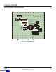
PCB Layout
For proper operation and minimum EMI, care must be
taken during printed circuit board layout. Figure 7 shows
the recommended component placement with trace,
ground plane and via locations. Note that large, switched
currents flow in the LT8608’s V
IN
pins, GND pins, and
the input capacitor (C1). The loop formed by the input
capacitor should be as small as possible by placing the
capacitor adjacent to the V
IN
and GND pins. When using
a physically large input capacitor the resulting loop may
become too large in which case using a small case/value
capacitor placed close to the V
IN
and GND pins plus a larger
capacitor further away is preferred. These components,
along with the inductor and output capacitor, should be
placed on the same side of the circuit board, and their
connections should be made on that layer. Place a local,
unbroken ground plane under the application circuit on
the layer closest to the surface layer. The SW and BOOST
nodes should be as small as possible. Finally, keep the FB
and RT nodes small so that the ground traces will shield
them from the SW and BOOST nodes. The exposed pad on
the bottom of the package must be soldered to ground so
that the pad is connected to ground electrically and also
Downloaded from Arrow.com.Downloaded from Arrow.com.Downloaded from Arrow.com.Downloaded from Arrow.com.Downloaded from Arrow.com.Downloaded from Arrow.com.Downloaded from Arrow.com.Downloaded from Arrow.com.Downloaded from Arrow.com.Downloaded from Arrow.com.Downloaded from Arrow.com.Downloaded from Arrow.com.Downloaded from Arrow.com.Downloaded from Arrow.com.Downloaded from Arrow.com.Downloaded from Arrow.com.