
Datasheet


LT8608/LT8608B
3
Rev. D
For more information www.analog.com
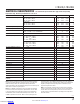
ELECTRICAL CHARACTERISTICS
The l denotes the specifications which apply over the full operating
temperature range, otherwise specifications are at T
A
= 25°C.
Note 1: Stresses beyond those listed under Absolute Maximum Ratings
may cause permanent damage to the device. Exposure to any Absolute
Maximum Rating condition for extended periods may affect device
reliability and lifetime. Absolute Maximum Ratings are those values beyond
which the life of a device may be impaired.
Note 2: The LT8608E is guaranteed to meet performance specifications
from 0°C to 125°C junction temperature. Specifications over the –40°C
to 125°C operating junction temperature range are assured by design,
characterization, and correlation with statistical process controls. The
LT8608I is guaranteed over the full –40°C to 125°C operating junction
temperature range. The LT8608H is guaranteed over the full –40°C to
150°C operating junction temperature range. High junction temperatures
degrade operating lifetimes. Operating lifetime is derated at junction
temperatures greater than 125°C.
Note 3: This IC includes overtemperature protection that is intended to
protect the device during overload conditions. Junction temperature will
exceed 150°C when overtemperature protection is active. Continuous
operation above the specified maximum operating junction temperature
will reduce lifetime.
PARAMETER CONDITIONS MIN TYP MAX UNITS
Feedback Reference Voltage MSOP Package
V
IN
= 6V, I
LOAD
= 100mA
V
IN
= 6V, I
LOAD
= 100mA
l
0.774
0.762
0.778
0.778
0.782
0.798
V
V
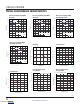
DFN Package
V
IN
= 6V, I
LOAD
= 100mA
V
IN
= 6V, I
LOAD
= 100mA
l
0.773
0.753
0.778
0.778
0.783
0.803
V
V
Feedback Voltage Line Regulation V
IN
= 4.0V to 40V
l
±0.02 ±0.06 %/V
Feedback Pin Input Current V
FB
= 1V
l
±20 nA
Minimum On-Time I
LOAD
= 1A, SYNC = 0V or LT8608 DFN
I
LOAD
= 1A, SYNC = 1.9V or LT8608B DFN
l
l
35
35
65
60
ns
ns
Minimum Off Time 93 130 ns
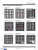
Oscillator Frequency MSOP Package
R
T
= 221k, I
LOAD
= 500mA
R
T
= 60.4k, I
LOAD
= 500mA
R
T
= 18.2k, I
LOAD
= 200mA
l
l
l
155
640
1.90
200
700
2.00
245
760
2.10
kHz
kHz
MHz
DFN Package
R
T
= 221k, I
LOAD
= 500mA
R
T
= 60.4k, I
LOAD
= 500mA
R
T
= 18.2k, I
LOAD
= 200mA
l
l
l
130
610
1.85
200
700
2.00
270
790
2.15
kHz
kHz
MHz
Top Power NMOS On-Resistance I
LOAD
= 0.5A 350 mΩ
Top Power NMOS Current Limit
l
2.1 2.9 3.9 A
Bottom Power NMOS On-Resistance 230 mΩ
SW Leakage Current V
IN =
36V
l
15 µA
EN/UV Pin Threshold EN/UV Rising
l
0.99 1.05 1.11 V
EN/UV Pin Hysteresis 50 mV
EN/UV Pin Current V
EN/UV
= 2V
l
±20 nA
PG Upper Threshold Offset from V
FB
V
FB
Rising
l
5.0 8.5 13.0 %
PG Lower Threshold Offset from V
FB
V
FB
Falling
l
5.0 8.5 13.0 %
PG Hysteresis 0.5 %
PG Leakage V
PG
= 42V
l
±200 nA
PG Pull-Down Resistance V
PG
= 0.1V 550 1200 Ω
Sync Low Input Voltage MSOP Only
l
0.4 0.9 V
Sync High Input Voltage INTV
CC
= 3.5V, MSOP Only
l
2.7 3.2 V
TR/SS Source Current MSOP Only
l
1 2 3 µA
TR/SS Pull-Down Resistance Fault Condition, TR/SS = 0.1V, MSOP Only 300 900 Ω
Spread Spectrum Modulation
Frequency
V
SYNC
= 3.3V, MSOP Only
l
0.5 3 6 kHz
Downloaded from Arrow.com.Downloaded from Arrow.com.Downloaded from Arrow.com.