
Datasheet


LT8608/LT8608B
8
Rev. D
For more information www.analog.com
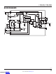
PIN FUNCTIONS
BST: This pin is used to provide a drive voltage, higher
than the input voltage, to the topside power switch. Place
a 0.1µF boost capacitor as close as possible to the IC. Do
not place a resistor in series with this pin.
SW: The SW pin is the output of the internal power
switches. Connect this pin to the inductor and boost
capacitor. This node should be kept small on the PCB for
good performance.
INTV
CC
: Internal 3.5V Regulator Bypass Pin. The internal
power drivers and control circuits are powered from this
voltage. INTV
CC
max output current is 20mA. Voltage on
INTV
CC
will vary between 2.8V and 3.5V. Decouple this
pin to power ground with at least a 1μF low ESR ceramic
capacitor. Do not load the INTV
CC
pin with external circuitry.
RT: A resistor is tied between RT and ground to set the
switching frequency. When synchronizing, the R
T
resistor
should be chosen to set the LT8608 switching frequency
equal to or below the lowest synchronization input.
SYNC (MSOP Only): External Clock Synchronization Input.
Ground this pin for low ripple Burst Mode operation at low
output loads. Tie to a clock source for synchronization to
an external frequency. Leave floating for pulse-skipping
mode with no spread spectrum modulation. Tie to INTV
CC
or tie to a voltage between 3.2V and 5.0V for pulse-skipping
mode with spread spectrum modulation. When in pulse-
skipping mode, the I
Q
will increase to several mA. There
is no SYNC pin in the LT8608 DFN package. The LT8608
DFN package internally ties SYNC to ground. The LT8608B
DFN package internally floats SYNC.
FB: The LT8608 regulates the FB pin to 0.778V. Connect
the feedback resistor divider tap to this pin.
TR/SS (MSOP Only): Output Tracking and Soft-Start Pin.
This pin allows user control of output voltage ramp rate
during start-up. A TR/SS voltage below 0.778V forces the
LT8608 to regulate the FB pin to equal the TR/SS pin volt-
age. When TR/SS is above 0.778V, the tracking function
is disabled and the internal reference resumes control of
the error amplifier. An internal 2μA pull-up current from
INTV
CC
on this pin allows a capacitor to program output
voltage slew rate. This pin is pulled to ground with a 300Ω
MOSFET during shutdown and fault conditions; use a series
resistor if driving from a low impedance output. There is
no TR/SS pin in the LT8608 DFN or LT8608B and the node
is internally floated.
PG: The PG pin is the open-drain output of an internal
comparator. PG remains low until the FB pin is within
±8.5% of the final regulation voltage, and there are no fault
conditions. PG is valid when V
IN
is above 3.2V, regardless
of EN/UV pin state.
V
IN
: The V
IN
pin supplies current to the LT8608 internal
circuitry and to the internal topside power switch. This pin
must be locally bypassed. Be sure to place the positive
terminal of the input capacitor as close as possible to the
V
IN
pins, and the negative capacitor terminal as close as
possible to the GND pins.
EN/UV: The LT8608 is shut down when this pin is low and
active when this pin is high. The hysteretic threshold volt-
age is 1.05V going up and 1.00V going down. Tie to V
IN
if the shutdown feature is not used. An external resistor
divider from V
IN
can be used to program a V
IN
threshold
below which the LT8608 will shut down.
GND: Exposed Pad Pin. The exposed pad must be con-
nected to the negative terminal of the input capacitor and
soldered to the PCB in order to lower the thermal resistance.
Downloaded from Arrow.com.Downloaded from Arrow.com.Downloaded from Arrow.com.Downloaded from Arrow.com.Downloaded from Arrow.com.Downloaded from Arrow.com.Downloaded from Arrow.com.Downloaded from Arrow.com.