
Datasheet
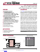
LT8614
10
For more information www.analog.com
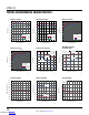
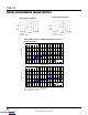
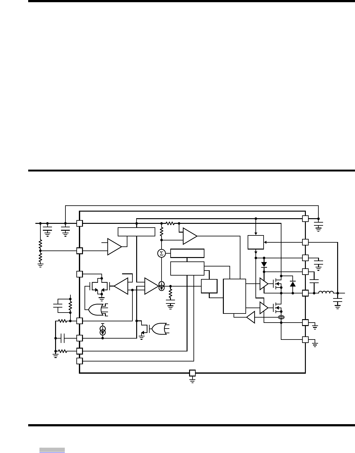
BLOCK DIAGRAM
+
+
–
+
–
SLOPE COMP
INTERNAL 0.97V REF
OSCILLATOR
200kHz TO 3MHz
BURST
DETECT
3.4V
REG
M1
M2
C
BST
C
OUT
V
OUT
8614 BD
SW
L
BST
8, 9, 21, 22
SWITCH
LOGIC
AND
ANTI-
SHOOT
THROUGH
ERROR
AMP
SHDN
±9%
V
C
SHDN
TSD
INTV
CC
UVLO
V
IN
UVLO
SHDN
TSD
V
IN
UVLO
EN/UV
1V
+
–
14
4
3
18
GND
INTV
CC
2
BIAS
1
V
IN2
13
GND1
6, 7
GND2
10, 11
PG
19
FB
R1C1
R3
OPT
R4
OPT
R2
R
T
C
SS
OPT
V
OUT
20
TR/SS
2.2µA
16
RT
15
SYNC/MODE
17
V
IN1
V
IN
C
IN1
C
IN3
C
VCC
C
IN2
PIN FUNCTIONS
SYNC/MODE (Pin 17): External Clock Synchronization
Input. Ground this pin for low ripple Burst Mode operation
at low output loads. Tie to a clock source for synchroniza-
tion to an external frequency. Apply a DC voltage of 3V or
higher or tie to INTV
CC
for pulse-skipping mode. When
in pulse-skipping mode, the I
Q
will increase to several
hundred µA. Do not float this pin.
GND (Pins 18): LT8614 Ground Pin. Connect this pin to
system ground and to the ground plane.
PG (Pin 19): The PG pin is the open-drain output of an
internal comparator. PG remains low until the FB pin is
within ±9% of the final regulation voltage, and there are
no fault conditions. PG is valid when V
IN
is above 3.4V,
regardless of EN/UV pin state.
FB (Pin 20): The LT8614 regulates the FB pin to 0.970V.
Connect the feedback resistor divider tap to this pin. Also,
connect a phase lead capacitor between FB and V
OUT
.
Typically, this capacitor is 4.7pF to 22pF.
SW (Exposed Pad Pins 21, 22): The exposed pads should
to connected and soldered to the SW trace for good ther-
mal performance. If necessary due to manufacturing limi-
tations Pins 21 and 22 may be left disconnected, however
thermal performance will be degraded.
Downloaded from Arrow.com.Downloaded from Arrow.com.Downloaded from Arrow.com.Downloaded from Arrow.com.Downloaded from Arrow.com.Downloaded from Arrow.com.Downloaded from Arrow.com.Downloaded from Arrow.com.Downloaded from Arrow.com.Downloaded from Arrow.com.