
Datasheet

LT8614
3
Rev. E
For more information www.analog.com
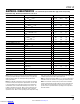
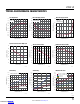
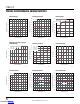
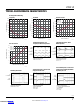
ELECTRICAL CHARACTERISTICS
Note 1: Stresses beyond those listed under Absolute Maximum Ratings
may cause permanent damage to the device. Exposure to any Absolute
Maximum Rating condition for extended periods may affect device
reliability and lifetime.
Note 2: The LT8614E is guaranteed to meet performance specifications
from 0°C to 125°C junction temperature. Specifications over the –40°C
to 125°C operating junction temperature range are assured by design,
characterization, and correlation with statistical process controls. The
LT8614I is guaranteed over the full –40°C to 125°C operating junction
temperature range. The LT8614H is guaranteed to meet performance
specifications from –40°C to 150°C operating junction temperature range.
The l denotes the specifications which apply over the full operating
temperature range, otherwise specifications are at T
A
= 25°C.
PARAMETER CONDITIONS MIN TYP MAX UNITS
Feedback Reference Voltage V
IN
= 6V, I
LOAD
= 0.5A
V
IN
= 6V, I
LOAD
= 0.5A
l
0.964
0.958
0.970
0.970
0.976
0.982
V
V
Feedback V
oltage Line Regulation V
IN
= 4.0V to 42V, I
LOAD
= 0.5A
l
0.004 0.02 %/V
Feedback Pin Input Current V
FB
= 1V –20 20 nA
INTV
CC
Voltage I
LOAD
= 0mA, V
BIAS
= 0V
I
LOAD
= 0mA, V
BIAS
= 3.3V
3.23
3.25
3.4
3.29
3.57
3.35
V
V
INTV
CC
Undervoltage Lockout 2.5 2.6 2.7 V
BIAS Pin Current Consumption V
BIAS
= 3.3V, I
LOAD
= 1A, 2MHz 9 mA
Minimum On-Time I
LOAD
= 1.5A, SYNC = 0V
I
LOAD
= 1.5A, SYNC = 3.3V
l
l
15
15
30
30
45
45
ns
ns
Minimum Off-T
ime 80 110 ns
Oscillator Frequency R
T
= 221k, I
LOAD
= 1A
R
T
= 60.4k, I
LOAD
= 1A
R
T
= 18.2k, I
LOAD
= 1A
l
l
l
180
665
1.85
210
700
2.00
240
735
2.15
kHz
kHz
MHz
T
op Power NMOS On-Resistance I
SW
= 1A 85 mΩ
Top Power NMOS Current Limit
l
5.7 8.5 10 A
Bottom Power NMOS On-Resistance V
INTVCC
= 3.4V, I
SW
= 1A 40 mΩ
Bottom Power NMOS Current Limit V
INTVCC
= 3.4V
l
4.5 6.9 8.5 A
SW Leakage Current V
IN
= 42V, V
SW
= 0V, 42V –1.5 1.5 µA
EN/UV Pin Threshold EN/UV Rising
l
0.94 1.0 1.06 V
EN/UV Pin Hysteresis 40 mV
EN/UV Pin Current V
EN/UV
= 2V –20 20 nA
PG Upper Threshold Offset from V
FB
V
FB
Falling
l
6 9.0 12 %
PG Lower Threshold Offset from V
FB
V
FB
Rising
l
–6 –9.0 –12 %
PG Hysteresis 1.2 %
PG Leakage V
PG
= 3.3V –40 40 nA
PG Pull-Down Resistance V
PG
= 0.1V
l
650 2000 Ω
SYNC Threshold SYNC Falling
SYNC Rising
0.8
1.6
1.1
2.0
1.4
2.4
V
V
SYNC Pin Current V
SYNC
= 6V –40 40 nA
TR/SS Source Current
l
1.5 2.2 2.9 µA
TR/SS Pull-Down Resistance Fault Condition, TR/SS = 0.1V 200 Ω
High junction temperatures degrade operating lifetimes. Operating lifetime
is derated at junction temperatures greater than 125°C.
Note 3: θ values determined per JEDEC 51-7, 51-12. See the Applications
Information section for information on improving the thermal resistance.
Note 4: This IC includes overtemperature protection that is intended to
protect the device during overload conditions. Junction temperature will
exceed 150°C when overtemperature protection is active. Continuous
operation above the specified maximum operating junction temperature
will reduce lifetime.
Downloaded from Arrow.com.Downloaded from Arrow.com.Downloaded from Arrow.com.