
Datasheet


LT8616
12
8616fa
For more information www.linear.com/LT8616
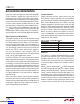
Achieving Ultralow Quiescent Current
To enhance efficiency at light loads, the LT8616 operates
in low ripple Burst Mode operation, which keeps the out
-
put capacitor charged to the desired output voltage while
minimizing the input quiescent current and output voltage
ripple. 1.7μA is supplied by V
IN1
to common bias circuits.
In Burst Mode operation the LT8616 delivers single small
pulses of current to the output capacitor followed by sleep
periods where the output power is supplied by the output
capacitor. While in sleep mode the LT8616 consumes 3μA.
As the output load decreases, the frequency of single cur
-
rent pulses decreases (see Figure 1a) and the percentage
of time that the LT8616 is in sleep mode increases, result-
ing in
much higher light load efficiency than for typical
converters.
By maximizing the time between pulses, the
converter quiescent current approaches 6.5µA for a typi
-
cal application when there is no output load. Therefore,
to optimize the quiescent current performance at light
loads, the current in the feedback resistor divider must
be minimized as it appears to the output as load current.
While in Burst Mode operation the current limit of the top
switch is approximately 400mA for
channel 1 (600
mA
for channel 2) resulting in output voltage ripple shown in
Figure 2. Increasing the output capacitance will decrease
the output ripple. As load increases from zero the switch
-
ing frequency
will increase but only up to the switching
frequency programmed by the resistor at the RT pin as
shown in Figure 1a. The output load at which the LT8616
reaches the programmed frequency varies based on input
voltage, output voltage, and inductor value.
For some applications it is desirable to select pulse-skipping
mode to maintain full switching frequency at lower output
load (see Figure 1b). See Pulse-Skipping Mode section.
FB Resistor Network
The output voltage is programmed with a resistor divider
between the output and the FB pin (R1 to R2 for channel 1,
R3 to
R4 for channel 2). Choose
the resistor values ac-
cording to:
R1= R2
V
OUT1
0.790V
–1
⎛
⎝
⎜
⎞
⎠
⎟
(1)
APPLICATIONS INFORMATION
Figure 1a. Frequency vs Load in Burst Mode Operation
Figure 1b. Minimum Load for Full
Frequency in Pulse-Skipping Mode
Figure 2. Burst Mode Operation
LOAD CURRENT (mA)
0
0
SWITCHING FREQUENCY (kHz)
800
700
600
500
400
300
200
100
200 350 400250
8616 F01a
30015010050
V
IN1
= V
IN2
= 12V
f
SW
= 700kHz
SYNC = 0V
CH2, 3.3V
CH1, 5V
V
IN
(V)
0
0
LOAD CURRENT (mA)
80
70
60
50
40
30
20
10
20 35 4025
8616 F01b
3015105
f
SW
= 700kHz
SYNC = 3V
CH2, 3.3V
CH1, 5V
5µs/DIV
V
OUT
(AC)
5mV/DIV
I
L
200mA/DIV
8616 F02
CH1 = 5V, 25mA
Downloaded from Arrow.com.Downloaded from Arrow.com.Downloaded from Arrow.com.Downloaded from Arrow.com.Downloaded from Arrow.com.Downloaded from Arrow.com.Downloaded from Arrow.com.Downloaded from Arrow.com.Downloaded from Arrow.com.Downloaded from Arrow.com.Downloaded from Arrow.com.Downloaded from Arrow.com.