
Datasheet


LT8616
13
8616fa
For more information www.linear.com/LT8616
APPLICATIONS INFORMATION
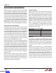
Figure 3. Switching Frequency vs R
T
Reference designators refer to the Block Diagram. 1% resis-
tors are recommended
to maintain output voltage accuracy.
If low input quiescent current and good light-load efficiency
are desired, use large resistor values for the FB resistor
divider. The current flowing in the divider acts as a load
current and will increase the no-load input current to the
converter, which is approximately:
I
Q
= 3µA +
V
OUT1
R1+ R2
⎛
⎝
⎜
⎞
⎠
⎟
V
OUT1
V
IN1
⎛
⎝
⎜
⎞
⎠
⎟
1
η
⎛
⎝
⎜
⎞
⎠
⎟
(2)
where 3µA is the quiescent current, the second term is
the current in the feedback divider reflected to the input
of channel 1 operating at its light load efficiency η. For a
3.3V application with R1 = 1M and R2 = 316k, the feedback
divider draws 2.5µA. With V
IN
= 12V and η = 70%, this
adds 1µA to the 3µA quiescent current resulting in 4µA
no-load current from the 12V supply.
Substitute R1 and R2 with R3 and R4 in the above equa
-
tion if V
IN1
and V
IN2
are connected to the same voltage.
Assuming channel 2 feedback divider contributes 2.5µA
to the quiescent current, then the total quiescent current
is 6.5µA.
For a typical FB resistor of 1MΩ, a 1.5pF to 10pF phase-
lead capacitor should be connected from V
OUT
to FB.
Setting the Switching Frequency
The LT8616 uses a constant frequency PWM architecture
that can be programmed to switch from 200kHz to 3MHz
by using a resistor tied from the RT pin to ground. Table 1
and Figure
3
show the necessary R
T
value for a desired
switching frequency.
The R
T
resistor required for a desired switching frequency
can be calculated using:
R
T
=
0.6
f
SW
2
+
42.6
f
SW
– 6.
1
(3)
where R
T
is in kΩ and f
SW
is the desired switching fre-
quency in MHz.
Table 1. SW Frequency vs R
T
Value
f
SW
(MHz) R
T
kΩ) f
SW
(MHz) R
T
kΩ)
0.2 221 1.6 20.5
0.3 143 1.8 17.8
0.4 105 2.0 15.4
0.5 80.6 2.05 14.7
0.6 66.5 2.2 13.3
0.7 56.2 2.4 11.8
0.8 47.5 2.6 10.3
1.0 37.4 2.8 9.31
1.2 29.4 3.0 8.25
1.4 24.3
The two channels of the LT8616 operate 180° out of
phase to avoid aligned switching edge noise and input
current ripple.
Operating Frequency Selection and Trade-Offs
Selection of the operating frequency is a trade-off between
efficiency, component size, and input voltage range. The
advantage of high frequency operation is that smaller induc
-
tor and
capacitor values may be used. The disadvantages
are
lower efficiency and a smaller input voltage range for
full frequency operation.
SWITCHING PERIOD (µs)
0
0
R
T
RESISTOR (kΩ)
120
140
160
180
200
220
100
80
60
40
20
240
1 2 3 4 5
8616 F03
Downloaded from Arrow.com.Downloaded from Arrow.com.Downloaded from Arrow.com.Downloaded from Arrow.com.Downloaded from Arrow.com.Downloaded from Arrow.com.Downloaded from Arrow.com.Downloaded from Arrow.com.Downloaded from Arrow.com.Downloaded from Arrow.com.Downloaded from Arrow.com.Downloaded from Arrow.com.Downloaded from Arrow.com.