
Datasheet


LT8616
19
8616fa
For more information www.linear.com/LT8616
APPLICATIONS INFORMATION
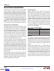
Figure 7. Reverse V
IN
Protection for
Tw o Independent Input Voltages
Pulse-Skipping Mode
Pulse-skipping mode is activated by applying logic high
(above 2.4V) or an external clock to the SYNC/MODE pin.
While in pulse-skipping mode, the oscillator operates
continuously and SW transitions are aligned to the clock.
During light loads, switch pulses are skipped to regulate
the output and the quiescent current per channel will be
several hundred µA. Full switching frequency is reached
at lower output load than in Burst Mode operation.
Shorted and Reversed Input Protection
The LT8616 will tolerate a shorted output. The bottom
switch current is monitored such that if inductor current
is beyond safe levels, turn on of the top switch will be
delayed until the inductor current falls to safe levels. A
fault condition of one channel will not affect the operation
of the other.
There is another situation to consider in systems where the
output will be held high when the input to the LT8616 is
absent. This may occur in battery charging applications or
in battery-backup systems where a battery or some other
supply is OR-ed with channel 1's output. If the V
IN1
pin is
allowed to float and either EN/UV pin is held high (either
by a logic signal or because it is tied to V
IN1
), then the
LT8616’s internal circuitry will pull its quiescent current
through its SW1 pin. This is acceptable if the system can
tolerate current draw in this state. If both EN/UV pins
are grounded the SW1 pin current will drop to near 1µA.
However, if the V
IN1
pin is grounded while channel 1
output is held high, regardless of EN/UV1, parasitic body
diodes inside the LT8616 can pull current from the output
through the SW1 pin and the V
IN1
pin, damaging the IC
V
IN2
is not connected to the shared internal supply and
will not draw any current if left floating. If both V
IN1
and
V
IN2
are floating, regardless of EN/UV pins states, no-load
will be present at the output of channel 2. However, if the
V
IN2
pin is grounded while channel 2 output is held high,
parasitic body diodes inside the LT8616 can pull current
from the output through the SW2 pin and the V
IN2
pin,
damaging the IC
Figure 7 shows a connection of the
V
IN
and EN/UV pins
that will allow the LT8616 to run only when the input
voltage is present and that protects against a shorted or
reversed input.
D1
LT8616
GND
D2
8616 F07
V
IN2
V
IN2
V
IN1
V
IN1
EN/UV1 EN/UV2
PCB Layout
For proper operation and minimum EMI, care must be taken
during printed circuit board layout. Figure 8 shows the
recommended component placement with trace, ground
plane and via locations. Note that large, switched currents
flow in the LT8616’s V
IN
pins, GND pins, and the input
capacitors (C
IN1
and C
IN2
). The loop formed by the input
capacitor should be as small as possible. When using a
physically large input capacitor the resulting loop may
become too large in which case using a small case/value
capacitor placed close to the V
IN
and GND pins plus a larger
capacitor further away is preferred. These components,
along with the inductor and output capacitor, should be
placed on the same side of the circuit board, and their
connections should be made on that layer. Place a local,
unbroken ground plane under the application circuit on
the layer closest to the surface layer. The SW and BOOST
nodes should be as small as possible. Finally, keep the FB
and R
T
nodes small so that the ground traces will shield
them from the SW and BOOST nodes. The exposed pad acts
as a heat sink and is connected electrically to ground
. The
exposed
pad of the TSSOP package is the only electrical
connection to ground and must be soldered to ground. To
keep thermal resistance low, extend the ground plane as
much as possible, and add thermal vias under and near
the LT8616 to additional ground planes within the circuit
board and on the bottom side.
Downloaded from Arrow.com.Downloaded from Arrow.com.Downloaded from Arrow.com.Downloaded from Arrow.com.Downloaded from Arrow.com.Downloaded from Arrow.com.Downloaded from Arrow.com.Downloaded from Arrow.com.Downloaded from Arrow.com.Downloaded from Arrow.com.Downloaded from Arrow.com.Downloaded from Arrow.com.Downloaded from Arrow.com.Downloaded from Arrow.com.Downloaded from Arrow.com.Downloaded from Arrow.com.Downloaded from Arrow.com.Downloaded from Arrow.com.Downloaded from Arrow.com.