
Datasheet


LT8616
20
8616fa
For more information www.linear.com/LT8616
APPLICATIONS INFORMATION
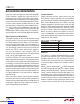
Figure 8. Recommended Layout
High Temperature Considerations
For higher ambient temperatures, care should be taken in
the layout of the PCB to ensure good heat sinking of the
LT8616. The exposed pad on the bottom of the package
must be soldered to a ground plane. This ground should
be tied to large copper layers below with thermal vias;
these layers will spread heat dissipated by the LT8616.
Placing additional vias can reduce thermal resistance
further. The maximum load current should be derated
as the ambient temperature approaches the maximum
junction rating. Power dissipation within the LT8616 can
be estimated by calculating the total power loss from an
efficiency measurement and subtracting the inductor loss.
The die temperature is calculated by multiplying the LT8616
power dissipation by the thermal resistance from junction
to ambient. The LT8616 will stop switching and indicate
a fault condition if safe junction temperature is exceeded.
Open Pins and Shorting Neighboring Pins
The LT8616 in TSSOP package is designed to tolerate
faults to each pin. Output voltages will stay at or below
regulation if adjacent pins are shorted or a pin is left float
-
ing. See Table 4 for pin fault behavior when the LT8616
in the TSSOP package is connected in the application
shown on Figure 9.
BOOST1V
IN1
EN/UV1
INTV
CC
RT
PG1
PG2
SYNC/MODE
TR/SS1
TR/SS2
SW1
LT8616
GND
FB1
BIAS
BOOST2
SW2
8616 F09
FB2
0.1µF
0.1µF
V
OUT1
5V, 1.5A
10pF
2 × 47µF
4.7µF 1M
5V, 3.3V, 700KHZ STEP-DOWN CONVERTER
200k
V
IN
12V
V
OUT2
3.3V, 2.5A
10nF
10µH
4.7µH
1M
316k
1M
1M
187k
56.2k
V
IN2
EN/UV2
4.7µF
5.6pF 47µF
1µF
Figure 9. See Table 4 for Open and Short Pin Behavior of this Application in the TSSOP Package
8616 F08
R2
NOTE: C
VCC
IS BELOW THE PACKAGE ON THE BACK SIDE
R1
L1
L2
R4
R3
C
FF1
C
BST1
C
BST2
C
FF2
C
IN2
C
IN1
R
T
R
PG1
C
OUT1
C
OUT2
R
PG2
1
2
3
4
5
6
7
8
9
10
11
12
13
14
TOP VIEW
FE PACKAGE
28-LEAD PLASTIC TSSOP
28
27
26
25
24
23
22
21
20
19
18
17
16
15
EN/UV2
PG2
SW2
SW2
SW2
BOOST2
NC
BOOST1
SW1
SW1
PG1
TR/SS1
FB1
FB1
TR/SS2
FB2
FB2
NC
V
IN2
NC
BIAS
INTV
CC
NC
V
IN1
NC
SYNC/MODE
EN/UV1
RT
29
GND
Downloaded from Arrow.com.Downloaded from Arrow.com.Downloaded from Arrow.com.Downloaded from Arrow.com.Downloaded from Arrow.com.Downloaded from Arrow.com.Downloaded from Arrow.com.Downloaded from Arrow.com.Downloaded from Arrow.com.Downloaded from Arrow.com.Downloaded from Arrow.com.Downloaded from Arrow.com.Downloaded from Arrow.com.Downloaded from Arrow.com.Downloaded from Arrow.com.Downloaded from Arrow.com.Downloaded from Arrow.com.Downloaded from Arrow.com.Downloaded from Arrow.com.Downloaded from Arrow.com.