
Datasheet
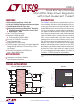

LT8616
9
8616fa
For more information www.linear.com/LT8616
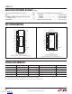
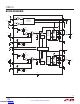
PIN FUNCTIONS
BIAS: The BIAS pin supplies the internal regulator when tied
to a voltage higher than 3.1V. For output voltages of 3.3V
and above this pin should be tied to the appropriate V
OUT
.
Connect a 1µF bypass capacitor to this pin if it is connected
to a supply other than V
OUT1
or V
OUT2
. Ground if unused.
BOOST1, BOOST2: The BOOST pins are used to provide
drive voltages, higher than the input voltage, to the internal
topside power switches. Place 0.1µF capacitors between
BOOST and its corresponding SW pin as close as possible
to the IC. BOOST nodes should be kept small on the PCB
for good performance.
EN/UV1, EN/UV2: The EN/UV pins are used to indepen
-
dently disable
each channel when pulled low and enable
when pulled high. The hysteretic threshold voltage is 1.03V
going up and 0.98V going down. Tie to V
IN
supply if the
shutdown feature is not used. External resistor dividers
from V
IN
can be used to program thresholds below which
each channel is disabled. Don’t float these pins.
FB1, FB2: The FB pins are regulated to 0.790V. Connect
the feedback resistor divider taps to the
FB pins. Also
connect phase lead capacitors between FB pins and V
OUT
nodes. Typical phase lead capacitors are 1.5pF to 10pF.
GND: The GND pins and exposed pad must be con
-
nected to the negative terminal of the input capacitors
and soldered to the PCB in order to lower the thermal
resistance.
INTV
CC
: The INTV
CC
pin provides power to internal gate
drivers and control circuits. INTV
CC
current will be sup-
plied from BIAS if V
BIAS
> 3.1V, otherwise current will be
drawn from V
IN1
. Decouple this pin to ground with at least
a 1μF low ESR ceramic capacitor. Do not load the INTV
CC
pin with external circuitry.
NC: The NC pins have no internal connection. Float NC
pins to increase fault tolerance or connect to ground to
facilitate PCB layout.
PG1, PG2: The PG pins are the open-drain outputs of the
internal power good comparators. Each channel's PG pin
remains low until the respective FB pin is within ±10% of
the final regulation voltage and there are no fault conditions.
RT: A resistor is tied between RT and ground to set the
switching frequency.
SW1, SW2: The SW pins are the outputs of
each chan-
nel's internal
power switches. Connect these pins to the
inductors and boost capacitors. SW nodes should be kept
small on the PCB for good performance.
SYNC/MODE: Ground the SYNC/MODE pin for low ripple
Burst Mode operation at low output loads. Tie to a clock
source for synchronization to an external frequency. Apply
a DC voltage of 2.4V or higher or tie to INTV
CC
for pulse-
skipping mode. When in pulse-skipping mode, the I
Q
will
increase to several hundred μA. Channel 1 will align its
positive switching edge to the positive edge of the external
clock and channel 2 will align its positive switching edge
to the negative external clock edge. Do not float this pin.
TR/SS1, TR/SS2: The TR/SS pins are used to soft-start
the two channels, to allow one channel to track the other
output, or to allow both channels to track another output.
For tracking, tie a resistor divider to the TR/SS pin from
the tracked output. For soft-start, tie a capacitor to TR/
SS. Internal 2μA pull-up currents from INTV
CC
charge
soft-start capacitors to create voltage ramps. A TR/SS
voltage below 0.79V
forces the
LT8616 to regulate the
corresponding FB pins to equal the TR/SS pin voltage.
When TR/SS voltages are above 0.79V, the tracking func
-
tion is disabled and the internal reference resumes control
of the error amplifiers. TR/SS pins are individually pulled
to ground with internal 250Ω MOSFETs during shutdown
and fault conditions; use series resistors if driving from
a low impedance output.
V
IN1
: V
IN1
supplies current to the LT8616's internal circuitry
and to channel 1's topside power switch. This pin must
be locally bypassed. Be sure to place the positive terminal
of the input capacitor as close as possible to the pin, and
the negative capacitor terminal as close as possible to the
GND pins. V
IN1
must be connected to 3.4V or above even
if only channel 2 is in use.
V
IN2
: V
IN2
supplies current to internal channel 2's topside
power switch. This pin must be locally bypassed. Be sure
to place the positive terminal of the input capacitor as close
as possible to the pin, and the negative capacitor terminal
as close as possible to the GND pins. Please note V
IN1
must be 3.4V or above to operate channel 2.
Downloaded from Arrow.com.Downloaded from Arrow.com.Downloaded from Arrow.com.Downloaded from Arrow.com.Downloaded from Arrow.com.Downloaded from Arrow.com.Downloaded from Arrow.com.Downloaded from Arrow.com.Downloaded from Arrow.com.