
Datasheet


LT8619/LT8619-5
13
Rev A
For more information www.analog.com
APPLICATIONS INFORMATION
Achieving Ultralow Quiescent Current
To enhance efficiency at light loads, the LT8619 enters into
Burst Mode operation, which keeps the output capacitor
charged to the desired output voltage while minimizing the
input quiescent current and output ripple voltage. In Burst
Mode operation the LT8619 delivers single small pulses of
current to the output capacitor followed by sleep periods
where the output power is supplied by the output capacitor.
While in sleep mode the LT8619 consumes less than 6μA.
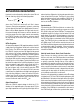
As the output load decreases, the frequency of single cur-
rent pulses decreases (see Figure1) and the percentage
of time the LT8619 is in sleep mode increases, result-
ing in much higher light load efficiency than for typical
converters. For a typical application, when the output is
not loaded, by maximizing the time between pulses, the
regulator quiescent approaches 6µA. Therefore, to opti
-
mize the quiescent current performance at light loads,
the current in the feedback resistor divider must be mini-
mized as it appears to the output as load current (See FB
Resistor Network section).
While in Burst Mode operation, the current limit of the
top switch is approximately 380mA resulting in output
voltage ripple shown in Figure2. Increasing the output
capacitance will decrease the output ripple proportionally.
As load ramps upward from zero, the switching frequency
will increase but only up to the switching frequency
programmed by the resistor at the RT pin as shown in
Figure1. The output load at which the LT8619 reaches
the programmed frequency varies based on input voltage,
output voltage, and inductor choice.
For some applications it is desirable for the LT8619 to
operate in pulse-skipping mode, offering two major dif-
ferences from Burst Mode operation. First, the minimum
inductor current clamp present in Burst Mode operation
is removed, providing a smaller packet of charge to the
output capacitor and reduce the output ripple voltage.
For a given load, the chip awake more often, resulting in
higher supply current compared to Burst Mode opera-
tion. Second is that full switching frequency is reached
at lower output load than in Burst Mode operation (see
Figure3). To enable pulse-skipping mode, leave the SYNC
pin floating. Tying the SYNC pin to INTV
CC
node enables
the programmed switching frequency at no load.
Figure1. Burst Frequency vs Load Current
8619 F02
V
OUT
(AC)
10mV/DIV
I
L
200mA/DIV
SW
10V/DIV
SW (ZOOM IN)
10V/DIV
I
L
(ZOOM IN)
200mA/DIV
V
OUT
(AC, ZOOM IN)
10mV/DIV
TOP = 20ms/DIV, BOT = 1μs/DIV
Figure2. Burst Mode Operation Waveform with
V
IN
= 12V, V
OUT
= 3.3V at No Load, R
T
= 66.5k,
L = 10μH, C
OUT
= 22μF
V
OUT
= 3.3V
f
OSC
= 700kHz
L = 10µH
V
IN
(V)
0
10
20
30
40
50
60
0
50
100
150
200
250
300
350
400
LOAD CURRENT (mA)
8619 F03
PULSE-SKIPPING MODE
Burst Mode OPERATION
V
IN
= 12V
V
OUT
= 3.3V
f
OSC
= 700kHz
L = 10µH
Burst Mode OPERATION
LOAD CURRENT (mA)
0.001
0.01
0.1
1
10
100
1k
0.01
0.1
1
10
100
1k
f
SW
(kHz)
8619 F01
Figure3. Minimum Load for Full Frequency Operation
vs V
IN
in Burst Mode Operation and Pulse-Skipping
Mode Setting
Downloaded from Arrow.com.Downloaded from Arrow.com.Downloaded from Arrow.com.Downloaded from Arrow.com.Downloaded from Arrow.com.Downloaded from Arrow.com.Downloaded from Arrow.com.Downloaded from Arrow.com.Downloaded from Arrow.com.Downloaded from Arrow.com.Downloaded from Arrow.com.Downloaded from Arrow.com.Downloaded from Arrow.com.