
Datasheet


LT8619/LT8619-5
14
Rev A
For more information www.analog.com
APPLICATIONS INFORMATION
FB Resistor Network
The output voltage is programmed with a resistor divider
between V
OUT
and the FB pin. Choose the resistor values
according to:
R1= R2
V
OUT
0.8V
– 1
⎛
⎝
⎜
⎞
⎠
⎟
Reference designators refer to the Block Diagram. 1%
resistors are recommended to maintain output voltage
accuracy.
If low input quiescent current and good light-load effi-
ciency are desired, use a large resistor value for the FB
resistor divider. The current flowing in the divider acts as
a load current, and will increase the no-load input current
to the converter, which is approximately:
I
Q
= 5.2µA +
V
OUT
R1+ R2
⎛
⎝
⎜
⎜
⎞
⎠
⎟
⎟
V
OUT
V
IN
⎛
⎝
⎜
⎜
⎜
⎞
⎠
⎟
⎟
⎟
1
η
⎛
⎝
⎜
⎜
⎞
⎠
⎟
⎟
where 5.2μA is the quiescent current of the LT8619 and
the second term is the current in the feedback divider
reflected to the input of the buck operating at its light load
efficiency, η. For a 3.3V application with R1 = 1M and
R2 = 316k, the feedback divider draws 2.5μA from V
OUT
.
With V
IN
= 12V and η = 85%, this adds 0.8μA to the 5.2μA
quiescent current resulting in 6μA quiescent current from
the 12V supply. Note that this equation implies that the
no-load current is a function of V
IN
; this is plotted in the
Typical Performance Characteristics section.
When using large FB resistors, a 4.7pF to 10pF phase
lead capacitor, C1, should be connected from V
OUT
to FB.
Setting the Switching Frequency
The LT8619 uses a constant frequency PWM architec-
ture that can be programmed to switch from 300kHz to
2.2MHz by using a resistor tied from the RT pin to ground.
The R
T
resistor required for a desired oscillator frequency
can be roughly obtain using:
R
T
=
50.07
f
OSC
– 5
where R
T
is in kΩ and f
OSC
is the desired switching fre-
quency in MHz.
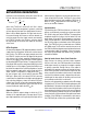
Table 1 and Figure4 show the typical R
T
value for a
desired oscillator frequency.
Table1. Oscillator Frequency vs R
T
Value (1% Standard Value)
f
OSC
(MHz) R
T
(kΩ) f
OSC
(MHz) R
T
(kΩ)
0.3 162 1.4 30.9
0.4 121 1.6 26.1
0.5 95.3 1.8 22.6
0.6 78.7 2.0 20.0
0.7 66.5 2.2 17.8
0.8 57.6
0.9 51.1
1.0 45.3
1.2 36.5
Figure4. Oscillator Frequency vs R
T
Value
Operating Frequency Selection and Trade-Offs
Selection of the operating frequency is a trade-off between
efficiency, component size, and input voltage range. The
advantage of high frequency operation is that smaller
inductor and capacitor values may be used. The disadvan-
tages are lower efficiency and a smaller input voltage range.
For force continuous mode operation, the highest oscil-
lator frequency (f
OSC(MAX)
) for a given application can be
approximately given by the 1st order equation:
f
OSC(MAX)
=
I
LOAD
R
SW(BOT)
+ V
OUT
t
ON(MIN)
V
IN
–I
LOAD
R
SW(TOP)
+I
LOAD
R
SW(BOT)
( )
Where V
IN
is the input voltage, V
OUT
is the output volt-
age, R
SW(TOP)
and R
SW(BOT)
are the internal switch on
resistance (~0.45Ω, ~0.22Ω, respectively) and t
ON(MIN)
R
T
(kΩ)
0
20
40
60
80
100
120
140
160
0.2
0.6
1.0
1.4
1.8
2.2
f
OSC
(MHz)
8619 F04
Downloaded from Arrow.com.Downloaded from Arrow.com.Downloaded from Arrow.com.Downloaded from Arrow.com.Downloaded from Arrow.com.Downloaded from Arrow.com.Downloaded from Arrow.com.Downloaded from Arrow.com.Downloaded from Arrow.com.Downloaded from Arrow.com.Downloaded from Arrow.com.Downloaded from Arrow.com.Downloaded from Arrow.com.Downloaded from Arrow.com.