
Datasheet


LT8619/LT8619-5
15
Rev A
For more information www.analog.com
APPLICATIONS INFORMATION
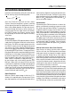
is the minimum top switch on-time at the loading condi-
tion as shown in Figure5. Figure6 shows the relation-
ship between the maximum input voltage vs the switching
frequency. If a smaller R
T
is selected, to ensure that the
regulator is switching at the higher frequency as illus-
trated in Figure4, the maximum input supply voltage has
to be lowered; and it needs to be further reduced if the
load is decreased or removed.
For forced continuous mode, if there is a momentarily V
IN
voltage surge higher than the voltage shown in Figure6,
resulting in minimum on-time operation, an overvoltage
comparator guards against transient overshoots as well
as other more serious conditions that may overvoltage the
output. When the V
FB
voltage rises by more than 3.75%
above its nominal value, the top MOSFET is turned off
and the bottom MOSFET is turned on. At this moment,
the output voltage continues to increase until the inductor
current reverses. The actual peak output voltage will be
higher than 3.75%, depending on external components
value, loading condition and output voltage setting. The
bottom MOSFET remains on continuously until the induc-
tor current exceeds the bottom MOSFET reverse current
or overvoltage condition is cleared. With high reverse cur-
rent, both top and bottom MOSFETs shut off till the next
clock cycle.
Low Supply Operation
The LT8619 is designed to remain operational during
short line transients when the input voltage may briefly
dip below 3.0V. Below this voltage, the INTV
CC
voltage
might drop to a point that is not able to provide adequate
gate drive voltage to turn on the MOSFET. The LT8619 has
two circuits to detect this undervoltage condition. A UVLO
comparator monitors the INTV
CC
voltage to ensure that it
is above 2.8V during startup; once in regulation, the chip
continues to operate as long as INTV
CC
stays above 2.65V.
If this UVLO comparator trips, the chip is shut down until
INTV
CC
recovers. Another comparator monitors the V
IN
supply voltage, add a resistor divider from V
IN
to EN/UV
to turn off the regulator if V
IN
dips below the undesirable
voltage.
The LT8619 is capable of a maximum duty cycle of greater
than 99%, and the V
IN
-to-V
OUT
dropout is limited by the
R
DS(ON)
of the top switch. In deep dropout, the loop
attempt to turn on the top switch continuously. However,
the top switch gate drive is biased from the floating boot-
strap capacitor C
B
, which normally recharges during each
off cycle; in dropout, this capacitor loses its refresh cycle
and charge depleted. A comparator detects the drop in
boot-strap capacitor voltage, forces the top switch off and
recharges the capacitor.
Figure5. Minimum On-Time vs Load Current
Figure6. Forced Continuous Mode Maximum Input
Voltage vs Switching Frequency
V
OUT
= 3.3V
f
SW
= 2MHz
L = 3.3µH
FORCED CONTINUOUS MODE
LOAD CURRENT (A)
0
0.2
0.4
0.6
0.8
1.0
1.2
0
10
20
30
40
50
60
70
80
MINIMUM ON-TIME (ns)
8619 F05
V
OUT
= 3.3V
L = 10µH
FORCED CONTINUOUS MODE
0.2A LOAD
f
SW
(MHz)
0.2
0.6
1.0
1.4
1.8
2.2
0
10
20
30
40
50
60
MAXIMUM V
IN
(V)
8619 F06
0.5A
LOAD
NO LOAD
High Supply Operation
For Burst Mode operation or pulse-skipping mode, V
IN
voltage may go as high as the absolute maximum rating
of 60V regardless of the frequency setting; however, the
LT8619 will reduce the switching frequency as necessary
to regulate the output voltage.
Downloaded from Arrow.com.Downloaded from Arrow.com.Downloaded from Arrow.com.Downloaded from Arrow.com.Downloaded from Arrow.com.Downloaded from Arrow.com.Downloaded from Arrow.com.Downloaded from Arrow.com.Downloaded from Arrow.com.Downloaded from Arrow.com.Downloaded from Arrow.com.Downloaded from Arrow.com.Downloaded from Arrow.com.Downloaded from Arrow.com.Downloaded from Arrow.com.