
Datasheet


LT8620
8
8620fa
For more information www.linear.com/LT8620
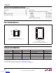
PIN FUNCTIONS
SYNC: External Clock Synchronization Input. Ground this
pin for low ripple Burst Mode operation at low output loads.
Tie to a clock source for synchronization to an external
frequency. Apply a DC voltage of 3V or higher or tie to
INTV
CC
for pulse-skipping mode. When in pulse-skipping
mode, the I
Q
will increase to several hundred µA. Do not
float this pin.
TR/SS: Output Tracking and Soft-Start Pin. This pin allows
user control of output voltage ramp rate during start-up. A
TR/SS voltage below 0.97V forces the LT8620 to regulate
the FB pin to equal the TR/SS pin voltage. When TR/SS
is above 0.97V, the tracking function is disabled and the
internal reference resumes control of the error amplifier.
An internal 2μA
pull-up current from INTV
CC
on this pin
allows a capacitor to program output voltage slew rate.
This pin is pulled to ground with an internal 220Ω MOS-
FET during shutdown and fault conditions; use a series
resistor if driving from a low impedance output. This pin
may be left floating if the tracking function is not needed.
RT: A resistor is tied between RT and ground
to set the
switching frequency.
EN/UV: The LT8620 is shut down when this pin is low and
active when this pin is high. The hysteretic threshold volt-
age is 1.00V going up and 0.96V going down. Tie to V
IN
if the shutdown feature is not used. An external resistor
divider from V
IN
can be used to program a V
IN
threshold
below which the LT
8620 will shut down.
V
IN
: The V
IN
pins supply current to the LT8620 internal
circuitry and to the internal topside power switch. These
pins must be tied together and be locally bypassed. Be
sure to place the positive terminal of the input capacitor
as close as possible to the V
IN
pins, and the negative
capacitor terminal as close as possible to the PGND pins.
NC
: No Connect. This pin is not connected to internal
circuitry.
SW: The SW pins are the outputs of the internal power
switches. Tie these pins together and connect them to the
inductor and boost capacitor. This node should be kept
small on the PCB for good performance.
BST: This pin is used to provide a drive voltage, higher
than the input voltage, to the topside
power switch. Place
a 0.1µF boost capacitor as close as possible to the IC.
INTV
CC
: Internal 3.4V Regulator Bypass Pin. The in-
ternal power drivers and control circuits are powered
from this voltage. INTV
CC
maximum output current is
20mA. Do not load the INTV
CC
pin with external cir-
cuitry. INTV
CC
current will be supplied from BIAS if
V
BIAS
> 3.1V, otherwise current will be drawn from V
IN
.
Voltage on INTV
CC
will vary between 2.8V and 3.4V when
V
BIAS
is between 3.0V and 3.6V. Decouple this pin to power
ground with at least a 1μF low ESR ceramic capacitor
placed close to the IC.
BIAS: The internal regulator will draw current from BIAS
instead of V
IN
when BIAS is tied to a voltage higher than
3.1V. For output voltages
of 3.3V to 25V, this pin should
be tied to V
OUT
. If this pin is tied to a supply other than
V
OUT
use a 1µF local bypass capacitor on this pin. If no
supply is available, tie to ground.
PG: The PG pin is the open-drain output of an internal
comparator. PG remains low until the FB pin is within
±9% of the final regulation
voltage, and there are no fault
conditions. PG is valid when V
IN
is above 3.4V, regardless
of EN/UV pin state.
FB: The LT8620 regulates the FB pin to 0.970V.
Connect the feedback resistor divider tap to this pin. Also,
connect a phase lead capacitor between FB and V
OUT
.
Typically, this capacitor is 4.7pF to 10pF.
GND: Ground. The exposed pad must be connected
to the
negative terminal of the input capacitor and soldered to
the PCB in order to lower the thermal resistance.
Downloaded from Arrow.com.Downloaded from Arrow.com.Downloaded from Arrow.com.Downloaded from Arrow.com.Downloaded from Arrow.com.Downloaded from Arrow.com.Downloaded from Arrow.com.Downloaded from Arrow.com.