
Datasheet


4
LTC1045
1045fc
V
OH
(Pin 1): High Level to which the Output Switches.
IN1 to IN7 (Pins 2 to 7): Six Comparator Inputs; Voltage
Range = V
–
to V
–
+ 18V.
V
TRIP2
(Pin 8): Trip Point for Last Two Comparators
(Inputs 5,6); Voltage Range = V
–
to V
+
– 2V.
V
TRIP1
(Pin 9): Trip Point for First Four Comparators
(Inputs 1 to 4); Voltage Range = V
–
to V
+
– 2V.
V
–
(Pin 10): Comparator Negative Supply.
V
OL
(Pin 11): Low Level to which the Output Switches.
I
SET
(Pin 12): This has three functions: 1) R
SET
from this
pin to V
–
sets bias current, 2) when forced to V
+
power is
shut off completely and 3) when forced to V
+
outputs are
latched.
DISABLE (Pin 13): When high, outputs are Hi-Z.
OUT6 to OUT1 (Pins 14 to 19): Six Driver Outputs.
V
+
(Pin 20): Comparator Positive Supply.
PIN FUNCTIONS
UUU
TEST CIRCUITS
50%
10%
90%
10%
t
OH
DISABLE
OUTPUTS
10pF
V
+
DISABLE
10k
V
OH
OUTPUT
1045 F03b
5V
–5V
t
OH
t
r
≤ 10ns
50%
10%
90%
90%
t
IH
DISABLE
OUTPUTS
10pF
V
+
DISABLE
10k
V
OL
OUTPUT
1045 F03a
5V
5V
0V
–5V
t
r
≤ 10ns
t
IH
–
+
50%
10%
90%
t
ACC
DISABLE
OUTPUTS
50pF
DISABLE
OUTPUT
1045 F03c
5V
–5V
t
ACC
t
r
≤ 10ns
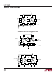
Figure 3. Three-State Output Test Circuit
Conditions: V
+
= V
OH
= 5V, V
–
= V
OL
= 0V
–
+
5V 5V
V
IN
V
TRIP
= 1.2V
V
+
V
–
V
OL
V
OH
OUTPUT
50pF
1045 F01
10%
t
r
= t
f
≤ 10ns
t
r
90%90%
10%
V
IN
OUTPUT
1.3V
1.2V
1.1V
5V
2.5V
0V
t
d
t
f
t
d
50%
50%
1045 F02
V
IN
I
SET
100mV
V
TRIP
V
TRIP
= 1.2V
V
IN
–100mV
5V
5V
0V
0V
t
HOLD
I
SET
t
SETUP
–
+
Figure 2. Latch Test Circuit
Figure 1. Response Time Test Circuit