
Datasheet


17
LTC1090
1090fc
Parallel Port Microprocessors
When interfacing the LTC1090 to an MPU which has a
parallel port, the serial signals are created on the port with
software. Three MPU port lines are programmed to create
the CS, SCLK and D
IN
signals for the LTC1090. A fourth
port line reads the D
OUT
line. An example is made of the
Intel 8051/8052/80C252 family.
Intel 8051
To interface to the 8051, the LTC1090 is programmed for
MSB first format and 10-bit word length. The 8051 gener-
ates CS, SCLK and D
IN
on three port lines and reads D
OUT
on the fourth.
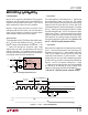
Hardware and Software Interface to Intel 8051 Processor
8051 Code
MNEMONIC DESCRIPTION
MOV PI,#02H Initialize port 1 (bit 1 is made
an input)
CLR P1.3 SCLK goes low
SETB P1.4 CS goes high
CONTINUE: MOV A,#0DH D
IN
word for the LTC1090 is
placed in ACC.
CLR P1.4 CS goes low
MOV R4,#08 Load counter
NOP Delay for deglitcher
LOOP: MOV C, P1.1 Read data bit into carry
RLC A Rotate data bit into ACC
MOV P1.2, C Output D
IN
bit to LTC1090
SETB P1.3 SCLK goes high
CLR P1.3 SCLK goes low
DJNZ R4, LOOP Next bit
MOV R2, A Store MSBs in R2
MOV C, P1.1 Read data bit into carry
CLR A CIear ACC
RLC A Rotate data bit into ACC
SETB P1.3 SCLK goes high
CLR P1.3 SCLK goes low
MOV C, P1.1 Read data bit into carry
RRC A Rotate right into ACC
RRC A Rotate right into ACC
MOV R3, A Store LSBs in R3
SETB P1.3 SCLK goes high
CLR P1.3 SCLK goes low
SETB P1.4 CS goes high
MOV R5,#07H Load counter
DELAY: DJNZ R5, DELAY Delay for LTC1090 to perform
conversion
AJMP CONTINUE Repeat program
APPLICATIO S I FOR ATIO
WUUU
Figure 5. Several LTC1090’s Sharing One 3-Wire Serial Interface
LTC1090
ANALOG
INPUTS
D
OUT
D
OUT
from LTC1090 stored in 8051 RAM
D
IN
SCLK
ACLK
CS
P1.1
P1.2
P1.3
ALE
P1.4
8051
B9R2
R3
*B9 is MSB in unipolar or sign bit in bipolar
MSB*
LSB
B8 B7 B6 B5 B4 B3 B2
B1 B0 000000
LTC1090 • AI14
LTC1090
3
3
210
CS
8 CHANNELS
OUTPUT PORT
SERIAL DATA
3-WIRE SERIAL
INTERFACE TO OTHER
PERIPHERALS OR LTC1090s
MPU
LTC1090
3
CS
8 CHANNELS
LTC1090
3
CS
8 CHANNELS